Information on Metal Layer Thickness and Metal Layer Thickness Measurements

Content Overview

Measurement by Eddy Current Testing | Testing Devices | Measurement | Deposition | Challenges | Sensors | How to Select the Measurement Technology

Metal Layer Thickness Measurement by Eddy Current Testing

Eddy current thickness gauges are applied across many industries measuring film thicknesses from a few nanometers to hundreds of micrometers or even millimeters. The underlying principle relies on the induction of eddy currents in metal films in all vertical present conductive elements. Each vertically stacked metal atom within a metal film contributes to the metal film's ability to transport electrical currents. This ability is described as sheet resistance and it correlates with metal thickness. Very thin metal films are analyzed by high frequency eddy current (< 100 MHz) sensors and very thick material films by low frequency eddy current sensors (> 10 kHz). Eddy current thickness gauges are calibrated directly to metal thicknesses of specific metal materials or use the metal thickness correlation to the sheet resistance. System deliveries are typically ready-to-use for various metal thickness measurement tasks. Especially, thick metal films are often measured by eddy current testing since optical measurements such as ellipsometry and reflectometry cannot be applied because they rely on a certain non-transparency. The user value derives especially from its robustness and its ability to measure in a contactless mode. The key benefits are:

  • Contact-free
  • Robustness
  • Well automatable for inline and in tool measurements
  • Ultra fast (20 ms / measurement)
  • Transmission mode and reflective mode gauges
  • High repeatability and accuracy
  • Measurement through encapsulation
  • Measurement of non-transparent metal films
  • Large measurement range 2 nm to 2 mm (depending on conductivity)

More about eddy current testing technology and suitable applications? Click here.

Types of Devices for Metal Layer Thickness Measurement

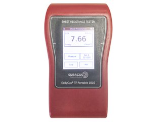
Portable metal layer thickness measurement device based on eddy current technology for the measurement of huge conductive samples
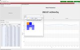
Sheet resistance measurement result of a glass with the portable measurement device EddyCus portable
Single point metal layer thickness measurement device based on eddy current technology for the measurement of conductive samples with a size of 200 mm x 200 mm
260 mOPS foil - drift compensation - manual mapping.jpg
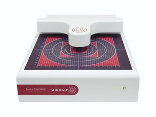
Fast and precise high quality table desk metal layer thickness mapping device based on eddy current technology for the measurement of conductive samples with a size of 300 mm x 300 mm such as wafers, glass with conductive layers, foils and others
High resolution mapping of an 8 in wafer with a 1mm pitch
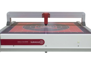
Inline metal layer thickness measurement system based on eddy current technology for the process quality and product quality monitoring of conductive products such as thin-films, coatings and materials
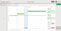
SURAGUS SUITE EC INLINE Measurement Screen.png

Metal Layer Thickness Measurement

Metal films are applied in thicknesses ranging from a few nanometers [nm] to larger micrometers [µm] or even millimeters [mm]. Their deposition is typically achieved by evaporation, sputtering, plating, atomic layer deposition (ALD) and other deposition techniques such as screen printing or laser metal deposition (LMD). Substrates are foils, glass, wafer, plastics, textiles or composites / compounds. Metals typically include copper, aluminum, nickel, chrome, zinc, gold, silver or alloys. Measurements during film deposition ("insitu" is a Latin phrase for during layer creation) are often not possible because thickness sensors cannot be installed in the direction of the deposition source since they would block the deposition material stream. Indirect measurements can be achieved by thickness "monitors" or deposition rate "controllers" such as quartz crystals thickness monitors but they suffer from larger offsets due to non-equal deposition rate on material and quartz. Such indirect measurements have a significant, non-constant offset which can be partially corrected by the "tooling factor". Therefore, sensors are installed directly after deposition, often "in-vacuo" (Latin phrase for in vacuum) or "ex-vacuo". Thickness sensors can be installed "in line" within the manufacturing process or offline as benchtop or portable testing solution.

List of Metals and Metal Alloys

Metals can be grouped into alkali metals, alkaline earth metals, basic metals and transition metals. Alkali metals are highly reactive elements and are therefore applied as compounds. Alkaline earth metals are less active but are also applied as compounds rather than in pure form. Basic metals, generally associated with the term "metal", conduct heat and electricity, have a metallic cluster and tend to be dense and ductile. Transition metals have an incompletely filled shell and therefore form multiple oxidation states. Some transition metals occur in pure or native form, including gold, copper, and silver.

Metals can be grouped as:

  • Alkali Metals (Lithium, Sodium, Potassium, Rubidium, Cesium, Francium)
  • Alkaline Earth Metals (Beryllium, Magnesium, Calcium, Strontium, Barium, Radium)
  • Basic Metals (Aluminum, Gallium, Indium, Tin, Thallium, Lead, Bismuth)
  • Transition Metals (Copper, Silver, Gold, Iron, Cobalt, Nickel, Zinc, Titanium, Chromium, Molybdenum, Vanadium, Manganese, Palladium, Cadmium)

Alloys can be grouped:

  • Aluminum Alloys (Al-Li, Alnico, Duralumin, Magnalium, Silumin)
  • Cobalt Alloys (Megallium, Stellite, Talonite)
  • Copper Alloys (Brass, Bronze , Copper-tungsten (copper, tungsten)
  • Gallium Alloys (Galinstan)
  • Gold Alloys (Electrum, Tumbaga, rose and white gold)
  • Iron or Ferrous Alloys (various types of Steel, Stainless steel and Ferroalloys)
  • Lead Alloys (Antimonial lead, Molybdochalkos, Solder)
  • Magnesium Alloys (Magnox, Elektron)
  • Nickel Alloys (Alumel, Chromel, Hastelloy, Inconel, Nisil
  • Silver Alloys (Britannia, Electrum, Goloid, Shibuichi)
  • Tin Alloys (Britannium, Pewter)
  • Titanium Alloys (Beta C,6al-4v)
  • Zinc Alloys (Brass, Zamak)
  • Zirconium Alloys (zircaloy)

Properties of Metal Films

Metal and alloy films usually consist of materials with different properties. The layer stack property is determined by these material properties and are finally achieved by its thickness and density:

Material and Layer Properties
  Material Property Layer Property
Electric

resistivity [ohm cm]

mobility [cm2⋅V-1⋅s-1]

sheet resistance [Ohm/sq]

carrier concentration [cm-3 ]

Dielectric

permittivity [F·m−1]

effective permittivity

Magnetic

permeability [[H·m-1] or [N·A-2]]

magnetic shielding @ frequency

Other related properties include emissivity and electromagnetic shielding at certain frequencies. Furthermore, metal thickness affects diffusion barrier (WVTR), grammage or area weight, acoustic impedance [Pa·s/m3] and absorption and for thin metal films also transmittance [%], reflectance [%] and diffusion / haze [%]. Many more properties apply. The properties listed here and their functions are often dependent on the metal thickness.

Metal Thickness and Sheet Resistance do Correlate

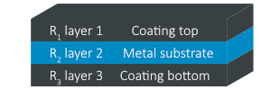
Eddy Current Technology mea­su­res through the entire layer stack and therefore provides the parallel resistance of the entire stack. Mul­ti­ple con­duc­ti­ve layers can be se­pa­ra­ted by mea­su­ring af­ter each coa­ting step and applying the standard formula. The thickness can be only calculated from the sheet resistance if the individual resistance of the layers have be determined by subsequent measurement.
 
Formula Sheet Resistance and Metal Thicknesses do Correlate.jpg
Visualization of a Layer Stack to Calculate the Metal Layer Thickness
  • Sheet resistance RS is defined as

Formula sheet resistance Rs.jpg
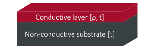
Here rho represents resistivity, and t represents thickness of conductive (metal) layer.
  • So thickness of conductive layer t is

Formula thickness of conductive metal layer.jpg
  • Since correlation between conductivity σ and resistivity ρ is as followed

Formula conductivity and resistivity.png
Layer stack conductive and non-conductive layer


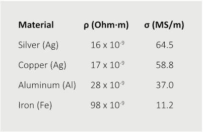
Material list with silver copper aluminum and iron and their resistivity per m and conductivity per meter

Deposition of Metal Films

Depending on its mechanical, electrical or optical properties as well as on the productivity requirements metals can be applied by vacuum and non-vacuum processes. Usually, highly precise applications such as precision optics require very smooth, dense and sensitive deposition processes such as sputtering. When it comes to thick layers in µm scale, evaporation is often commonly used. Other vacuum processes are ALD, CVD and PECVD. Non-vacuum processes are atmospheric plasma, wet or wet-chemical processes.

Metal Deposition by Plating

Electroplating or electroless plating are wet deposition processes. Electric plating requires an electric current for binding metals onto the surface. While in a bath with metal particles and chemicals, an electric current is applied to the substrate which leads to a deposition process. In contrast, electroless plating is based on a auto-catalytic process that does not require any electric current. The substrate is being treated with chemicals and the catalytic solution which finally causes oxidation. Hence, metal particles bind to substrate surface.

Materials

  • Metals
  • Alloys

Applications

  • Corrosion protection
  • Diffusion barriers
  • Conductive circuit elements
  • Via-holes in semiconductor
  • Through-hole connections for PCB

Metal Deposition by Evaporation

Evaporation is a physical vapor deposition process (PVD). Evaporation is based on vaporizing a material in a vacuum environment by heating it beyond its melting or subliming temperature. Compared to magnetron sputtering, evaporation in principle is a high deposition rate process that generally achieves lower densities and lower uniformity, unless ion-assist mask technology or planetary are not being used. Hence, in large substrate width uses cases with high optical requirements the evaporation process could be limiting. Depending on the melting point evaporation can be done by resistive heaters or electron beam.

Applications

  • Batteries
  • Fuel cells
  • Capacitors
  • OLED
  • Precision optics
  • Display industry
  • Thin film solar
  • Semiconductor

Materials (characterized by low and high melting points)

  • Metals
  • Non-metals
  • Alloys
  • Dielectrics

Metal Deposition by Magnetron Sputtering

Magnetron sputtering is a physical vapor deposition process (PVD). It requires a magnetically confined plasma process in a vacuum environment where positively charged ions collide with a negatively charged target material. In doing so the target material ejects atoms which then adhere to a substrate, such as glass, Si, plastics etc. Compared to the evaporation process, magnetron sputtering is a low deposition rate process that achieves a high homogeneity especially across large substrate widths. Sputtering can be applied on coupon (10 mm x 10 mm) or wafer level up to substrate widths of 3,300 mm. Depending on customers requirements (thin film quality, machine productivity) different mechanical layouts and operation modes can be adopted. Operating modes include RF/ HF, DC, pulsed DC, DC/DC, DC/RF. Configurations with single planar targets, confocal, rotatable targets, dual rotatable targets and facing targets are common.

Typical applications are

  • Flat Panel Displays
  • Optical Discs
  • Automotive & Architectural Glass
  • Decorative Coatings
  • Hard Coatings
  • Solar Cells
  • Optical Communications
  • Magnetic Data Storage Devices
  • Semiconductors
  • Electron Microscopy

Typical coatings are

  • Aluminum Al, Aluminum-Titanium Al-Ti, Aluminum oxide Al2O3
  • Cadmium Telluride CdTe, Cadmium Selenide CdSe, Cadmium Sulphide CdS
  • Chromium Cr, Chromium-Molybdenum Cr-Mo, Chromium-Titanium Cr-Ti, Chromium-Tungsten Cr-W,  Chromium-Vanadium Cr-V, Chromium-Molybdenum-Tantalum Cr-Mo-Ta
  • Cobalt Co, Cobalt-Chromium-Tantalum-Boron, Cobalt-Iron-Boron Co-Fe-B
  • Copper Cu, Copper alloys
  • Indium Tin oxide (ITO, In2O3-SnO2)
  • Iron Fe, Iron-Cobalt-Boron Fe-Co-B, Iron-Tantalum-Carbon Fe-Ta-C
  • Gold Au, Gold-Silver Au-Ag, Gold-Palladium Au-Pd, Gold-Platinum Au-Pt
  • Molybdenum Mo, Molybdenum-Tungsten Mo-W, Molybdenum-Niobium Mo-Nb, Molybdenum-Silicon Mo-Si
  • Niobium Nb,
  • Nickel Ni, Nickel-Chromium Ni-Cr, Nickel alloys
  • Platinum Pt, Platinum-Palladium Pt-Pd, Platinum-Silver Pl-Ag
  • Ruthenium Ru, Ruthenium-Aluminum Ru-Al
  • Silicon Si, Silicon-Aluminum Si-Al, Silicon dioxide SiO2
  • Silver Ag
  • Tantalum Ta, Tantalum pentoxide Ta2O5, Tantalum-Silicon TaSi
  • Tin Sn
  • Titanium Ti, Titanium oxide TiOx, Titanium-Aluminum Ti-Al, Titanium-Tungsten Ti-W
  • Terbium-Iron-Cobalt Tb-Fe-Co and many other alloys.
  • Tungsten W, Tungsten-Silicon W-Si
  • Zinc Zn, Zinc sulfide ZnS, Zinc-Aluminum Zn-Al
  • Zirconium Zr, Zirconium boride ZrB2

Atomic Layer Deposition (ALD)

ALD is a chemical vapor deposition process (CVD). Compared to magnetron sputtering, ALD is a low deposition rate process where typically Ångstrom thick films in single digit scale are being deposited. At least two chemical vapors or precursors react on the substrate applying a thin film. Due to its low deposition rate it produces dense and smooth layers. In recent years, ALD was developed to fit the requirements of industrial scale processes such as R2R and spatial ALD.

Materials that are being applied by ALD are:

  • Metals
  • Metal oxides, nitrides, sulfides, carbides
  • Polymers
  • Others

Applications

  • Barrier layers
  • Microelectronics
  • Semiconductor

How to Select a Layer Thickness Measurement Technology

Layer Thickness Measurement Technologies

Clustering of technology

  • Direct vs. indirect methods
  • Destructive vs. non-destructive methods
  • Often destructive methods allow the direct measurement whereas most non-destructive (non-contact) methods use indirect relations and, therefore, require calibration or reference parameters.

Considering material stack e.g. substrate separation

  • Conductive and non-conductive
  • Transparent and semi- or non-transparent
  • Reflective and non-reflective
  • Ferromagnetic and non-ferromagnetic

Challenges of Layer Thickness Measurement

Challenges of metal layer thickness measurement involve:

  • Multi-layer-thickness measurement
  • Ultra-thin layer thickness measurement
  • Boundary layer thickness measurement

Thickness measurements can often be performed using different techniques. Typically, there are many influencing variables from substrates and layer properties to environment and measurement type which should be taken into close consideration.

Layer Thickness Sensors

Thickness sensors differentiate materials using various technologies. Common techniques involve surface profilers, ellipsometry, dual polarization interferometry and scanning electron microscopy to analyze the cross-sections of the samples.

Thickness Gauging Methods

The data displayed in the following comparison tables is obtained from "Nitzsche, K.: Schichtmeßtechnik. Vogel, 1997."

Eddy Current Thickness Gauging Methods

Eddy current measurement is a reliable non-contact testing method. It is applicable to a wide range of different tasks, such as detection of surface damages, vibration and deformation measurement, measurement of material properties like electrical conductivity and magnetic permeability as well as proximity sensing. Proximity sensing and sensing of conductivity allows for a very precise determination of the thickness of various layer/substrate systems.

  • Requires conductive coating
  • Very large measurement range
  • Fast measurement method
  • Mature method
  • Medium to high costs

Eddy Current Gauging Methods for metal layer Thickness Measurement

Mechanical Thickness Gauging Methods

Dial gauges and comparator gauges are relatively simple tools which play a subordinate role. A tip scans the surface using the power of gravity or of a spring and then converts the jump of the tip at a step into the thickness. Similar methods are profile methods that are primarily used for roughness investigations. A diamond tip scans the surface and converts the movement into an amplified electrical signal. Advantages of those methods are that they are direct measurement methods with great reproducibility.

They are inexpensive, there are no requirements towards the layer system and roughness can be erased by averaging. The main disadvantage is the need for a step and the contact to the layer that may cause elastic or plastic deformation. Moreover, they are not applicable for in-situ measurements.

  • Typically requires physical contact and a physical step
  • Well known technology
  • Inexpensive

Mechanical Gauging Methods for metal layer Thickness measurement

Thickness Determination by Weight Measuring

Knowing the layer area and the density of the layer material allows the determination of thickness by weight measuring. This is achieved either by measuring the weight difference of the structure of interest or by investigating the weight of a reference structure. Analysis and micro scales or other special disposition weight measuring methods are very precise, but allow very low loads and an in-situ application is difficult. A common and even more precise and in-situ applicable method is the quartz monitor method. A quartz in the chamber next to the substrate is coated under the same condition. The quartz alters its oscillation characteristics depending on its weight which is monitored and evaluated. It is an extremely precise method that is also suitable for coating sequences. Another approach is the weight measurement of the consumed vapored material. It is a simple but not very precise method. Furthermore, there are also chemical quantitative analysis which determines thickness by measuring the duration of a chemical reaction for detachment of the layer. The coulometric method determines the thickness in a reverse electrolysis by measuring the changing potential. It is very precise but destroys the layer so it is mainly used for lab applications.

  • Medium costs
  • Inline and insitu applications
  • Mature technology

Layer Thickness Determination by Weight Measuring

Radiometrical Thickness Gauging Methods

The interaction of ionized or radioactive emission with layer matter provides plenty of information on material characteristics. Depending on material and thickness, different emission types are applied. Commonly used are alpha, beta, gamma, X-ray or electron emission. Effects are transmission, absorption and back scattering. All approaches use a source and a receiver. Common receivers are ionization chambers, radiation counters, scintillator counters or crystal counters. A high emission supports a high resolution but increases hazardous radiation. The radioactive transmission approach analyzes, similar to the optical transmission approach, the weakening intensity caused by the sample. An essential condition is that the proportion of absorption due to the substrate is not too high so that variations due to the layer can still be analyzed. Furthermore, a calibration curve is required and both sides of the sample are occupied for measurements. The Tracer method mixes radioactive isotopes into the layer and determines the thickness by the radiation intensity. In the Beta-Back-Scattering method a sample is bombarded with a tilted collimated beam of electrons from a weak radioactive beta source. As reflected primary radiation is blocked by an obstacle, only radiation emitted by the layer is received and then referenced to the thickness. Another well established approach is the Fluorescence method. Here, electric transitions caused by x-ray, gamma or beta radiation in the atomic shell emit light which is characteristic for every chemical element. Hence, next to thickness gauging also qualitative characterizations are possible. Although all radioactive methods have a high sensitivity, users have to consider potential health issues.

  • Variety of testing methods and setups are available
  • Mature technology
  • Medium to high costs
  • Requires safety measure to cope with radioactive tools

Radiometrical Gauging Methods for Layer  Thickness Measurement

Magnetic Thickness Gauging Methods

Magnetometers can be used for all non-ferromagnetic coatings on ferromagnetic substrates. They are often used for rapid quality assurance of galvanic layers (like zinc, copper or aluminum) on steel or iron. Magnetometers evaluate magnetic fields induced by coils that are influenced by the distance to the substrate. Since this technique requires to contact the surface of the test material, it may impact the surface. Despite the simplicity of the approach, there are many issues to consider when contacting a layer as the probe position influences the measurement. Issues are too small samples, non-planar surfaces, roughness and misbalance of the probe. Carried out properly, the method allows thickness determination from few μm to few mm, if referenced to calibration samples. Measurements can be done with various arrangements of one or more coils following the induction law and analyzing various effects. Common are fluxgate magnetometers, rotating coil magnetometers or hall effect magnetometers. In the most basic form, the fluxgate magnetometer comprises two coils which share the same core. In a magnetically neutral background, the input and output currents match but if the core is exposed to a magnetic background field, then the signal changes due to varying saturation efforts. The rotating coil magnetometer induces a sine wave in a rotating coil and evaluates the amplitude of the signal. A hall voltage can be measured when an ashlar conductor or semiconductor is transduced by a current accompanied by a perpendicularly arranged magnetic field. The evaluation of the caused hall voltage provides an insight into the electrical properties, charge carrier density and mobility and, hence, the conductivity. There are many physical effects for consideration but especially for silicon and germanium layers, which have a high hall coefficient, this method allows reliable measurements without the need for references. A further approach is the adhesion strength measurement which analyzes the strength during the detachment of a permanent magnet and converts this into the thickness.

  • Mature technologies
  • Low to medium high cost
  • Require magnetic layers
Magnetic Gauging Methods for Layer Thickness Measurement

Optical Thickness Gauging Methods

Microscopy methods demand, with a few exceptions, an edge. Thus, a cut into the material is required which can be archived, e.g., by focused ion beam or etching. There are many ways to determine the thickness using microscopy like using depth of focus, scaling with multimeter, light cutting methods or a scan with SEM. Interferometric methods also require a step unless the material is transparent. Interference refers to the interaction of two or more waves that are correlated or coherent with each other.

Interference techniques have been well investigated and developed. Major approaches are transmission interference, incident light interference and interphako interference. Irradiation techniques evaluate the intensity of the perpendicular light beam that is transmitted through the sample. This approach analyzes the reflectance and absorptance behavior of transparent and semitransparent layers. It is a widely applied method for coated foils in the packaging industry. Ellipsometry analyses the change of polarization when parallelized light pervades a transparent or semitransparent layer. Most common is the application in reflection mode. The advantage for in-situ applications is that the area above the sample is not blocked and, hence, a measurement during the coating process is possible. Furthermore, it is an extremely precise, very fast, non-destructive, contact-free and in-situ applicable method which does not require reference measurements. Disadvantageous is the limitation to transparent layers, sensitivity towards micro structural effects, micro roughness and micro criticality.

  • Limitation to transparent layers (thin metal layers)
  • Sensitivity to micro structural effects and micro roughness
  • Suitable for inline application
  • Medium to high costs

Optical Gauging Methods Layer Thickness Measurement

Testing Devices for Metal Layer Thickness Measurements

Industry and R&D laboratories have different requirements when it comes to the number of samples and measurement tasks per day, measurement point density and its automation level. In result, four key testing types are commonly applied:

Contact

For product requests contact us by using the

For a prompt and informative response, please describe your measurement task (material, sample dimensions, expected measurement range) and provide your phone number.

By sending this form, I permit SURAGUS GmbH to process my data for contacting me. For more details see our Imprint & Privacy Policy