Sheet Resistance Measurement
Content Overview
Table of Contents
Sheet Resistance Measurements by Eddy Current
Eddy current gauges are applied for sheet resistance testing since 30 years. Its accuracy and its ability to measure in contactless mode has a special user value. Key benefits of eddy current resistance testing are:
- Non-contact mode
- Ultra-fast (20 ms / measurement)
- High repeatability and accuracy
- Large distances from sensor to substrate
- Transmission mode and reflective mode
- Measurement through encapsulation
- No wearing
- Large measurement range from 0.1 mOhm/sq to 100 kOhm/sq (9 decades)
Sheet Resistance Measurement Devices from SURAGUS
Handheld Devices
for Single Point Measurements
Handheld eddy current devices are designed for fast, random sampling of product quality—commonly used at goods receipt or for inspecting particularly large components after production.
To perform a measurement, the device is placed on the target surface. Press the “Measure” button, and within one second, the result is displayed.
Each measurement provides a precise value at the specific point tested—offering instant, reliable feedback wherever flexibility and speed are essential.
Benchtop Tools
for Single Point Measurements
Our handheld systems are ideal for quick, spot-check measurements—whether at goods receipt, during in-process inspection, or for large-format components where fixed setups are impractical.
Simply place the handheld unit on the surface to be measured, press the “Measure” button, and within one second, the measurement value appears on the display.
Each reading represents the precise value at the measurement point—giving you rapid, reliable feedback wherever you need it.
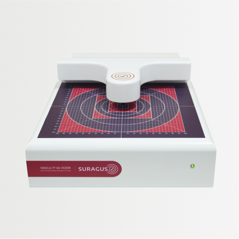
Imaging Tools
for Full Area Images
Our technology delivers highly detailed, full-surface information about product quality—enabling meaningful conclusions about process quality and stability. This data supports targeted optimization of both the manufacturing process (e.g., resource efficiency, throughput speed) and the product itself (e.g., improved homogeneity, compliance with minimum specifications).
For measurement, the sample is placed centrally on the measurement field. Prefabricated holders—such as those for wafers—ensure precise, centered positioning. Simply insert the sample, close the flap, and press “Start Measurement.”
The result: a high-resolution false-color map of the entire layer, generated from thousands of individual measurement points. This visualization gives you actionable insights at a glance.
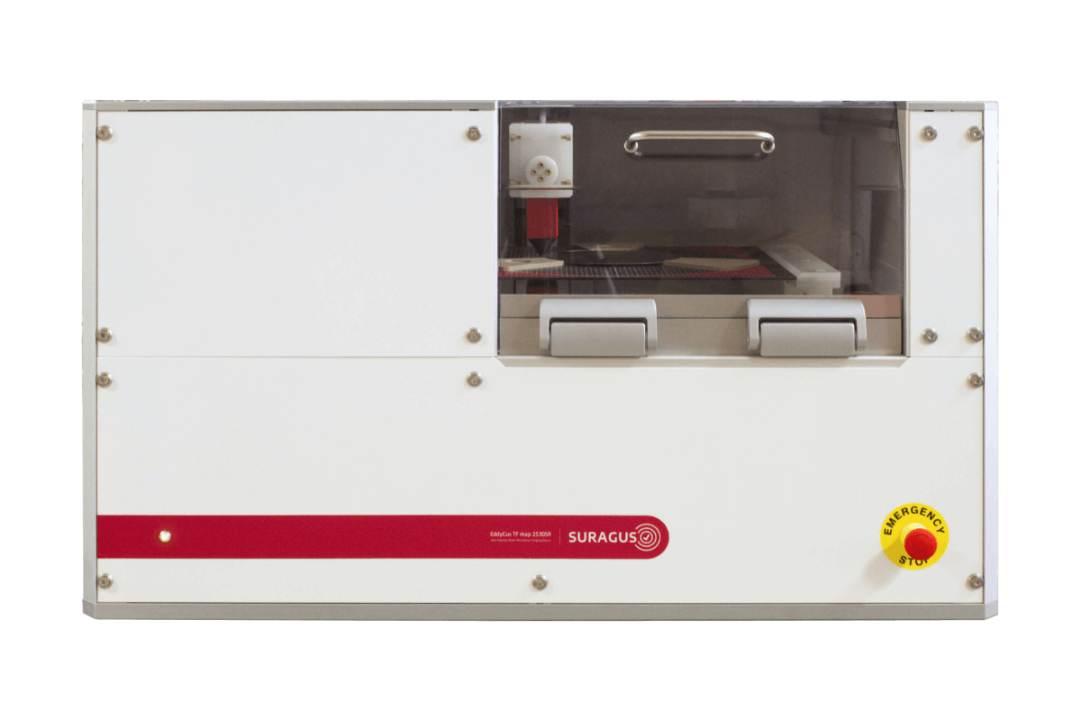
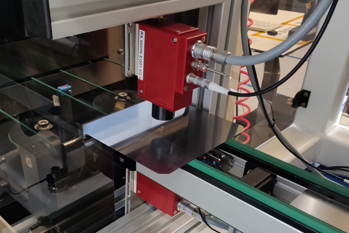
Inline Systems
for Continuous Single Point Measurements
Our inline systems enable continuous acquisition of data on both process quality and product characteristics—before, during, or after a production step. This real-time monitoring is a foundation for production automation, which relies on precise and reliable sensor data.
The system is seamlessly integrated into your existing production line. Once the operator initiates measurement, all data is automatically recorded and stored in a centralized database.
Depending on the system configuration, the output includes one or more line profiles—either centered or positioned at critical points across the layer—providing clear insight into quality trends and process stability in real time.
Sheet Resistance Measurements by Eddy Current
Sheet resistance (Rs or R), also known as sheet rho, is a measure for the electrical resistance of thin layers. It is related to the resistivity of both material and layer thickness. The sheet resistance value (typically stated in Ω/sq or Ohm/sq or Ohm per square or OPS) provides a measure for the electrical characteristics of conductive and and semi-conducting layers. It is the main physical parameter for describing the electrical performance of electrodes. The sheet resistance Rs correlates with the material thickness if the bulk resistivity can be assumed to be constant. The formula is
ρ = RS · t where ρ is the resistivity; RS is the sheet resistance; and t is the thickness of the material
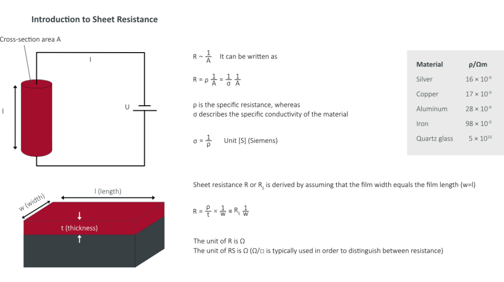
Sheet resistance describes the ability of a square layer to conduct a certain current. This characteristic is the most important quality parameter for surface electrodes and is determined during layer deposition process or for quality assurance of conductive thin films.
Contact Us For More Information
Sheet Resistance Measurement Unit
Even though the correct physical unit of sheet resistance or sheet resistivity is Ohm, the unit most commonly used is Ohm/ sq.
The sheet resistance is specified in Ohm/sq or OPS, in order to achieve a differentiation for the general resistance, which is indicated in Ohm. Very thick layer and highly conductive layers are often described in mOhm/sq and low conductive material is often described using kOhm/sq or MOhm/sq.
Sheet Resistance Measurement Techniques
There are two different modes to measure the sheet resistance – non-contact and contact. Non-contact sheet resistance measurement is possible with the following techniques:
| Contact | Non-contact |
| Two-point-probe | Eddy current |
| Four-point-probe | |
| Hall effect | |
| Van der Pauw |
Learn more about Eddy Current current based sheet resistance testing in our technology section.
Sheet Resistance Measurement by Four-Point-Probe Testing (2PP/ 4PP)
The four-point-probe method works by contacting four equally-spaced, co-linear probes to the material. This method is known as a four-point probe method. A direct current (DC) is driven between the outer two probes whereas the voltage is measured between the inner two probes. Often a geometric correction factor is required when measuring on small samples or close to edges, where current pathways are affected by the sample geometry. The most accurate values can be obtained in the center of samples.
Sheet Resistance Measurement by Eddy Current Testing (EC)
Eddy current sheet resistance testing devices drive an alternating current (AC) through coils to generate a (primary) electromagnetic field that induces so called (eddy) currents in conductive materials. The induced currents in the test object operate with the same AC frequency as applied to the induction coils resulting in a secondary field which is opposed to the primary field. The sum of both fields or the change in fields describes the sheet resistance.
Comparison of 4PP and EC Sheet Resistance Testing
Eddy Current, 4PP, Hall-Effect and Van-der-Pauw methods are electrical testing methods applicable for testing of the electrical parameter sheet resistance. Hall-Effect and Van-der-Pauw measurements are applied on R&D level since both methods typically require sample preparation. Industry is commonly using contact 4PP and non-contact Eddy Current (EC) measurements which do not require sample preparation. The key differences are summarized in the next image.
| Eddy Current | Four Point Probe | |
|---|---|---|
| Mode | Non-contact | Contact |
| Measurement Range | 0.1 mOhm/sq to 200 kOhm/sq | 1 mOhm/sq to 10 kOhm/sq |
| Time | real time | few seconds (incl. contact establishment |
| Application Range |
Imaging with 1 mm pitch Inline 50 measurements / sec |
Imaging with given number of measurement points Inline |
| Wearing Costs | None | Test prods |
| Contamination | None |
Possible contamination (Semiconductor, OLED industry) |
| Physical Impact | None | Possible layer damage |
| Measured Layer |
Hidden layers Conductive multi layer systems |
Only top layer |
| Provenance | >30 years | >70 years |
| Calibration | By manufacturer or user | By manufacturer or user |
Eddy Current Testing allows accurate measurement without impacts due to inhomogeneous contact quality, without damaging any sensitive surface or inducing artifacts due to contacting. Furthermore, it allows the accurate measurement of inaccessibly buried or encapsulated layers. Applying non-contact technology, there is no wear of needles or tips, which typically causes high replacement costs in common 4-point-probe mapping systems. A further significant advantage is the short measurement time. A measurement takes only a few milliseconds for each measurement and no time for contacting the sample is needed. This also allows to measure inline during production or “on the fly” in mapping systems. In result, the eddy current sheet resistance mapping systems measure thousands of positions in a couple of seconds. No interpolation between measurements points – as typical in 4-point-probe mapping systems – is required. Hence, defects and non-uniform areas can be identified.
Sheet Resistances Applications and Measurement Ranges
Sheet resistance is a key quality parameter in architectural glass, photovoltaics, display, OLED, touch panel sensors, packaging, semiconductor and many more industries. The following table provides an overview of typical sheet resistance values across different applications.
| Application | Main Sheet Resistance Range in Ohm/ sq |
| Architectural Glass (LowE) | 1 – 10 |
| Transparent Electrodes in PV and Smart Glass | 5 – 50 |
| Transparent Electrodes in OLED | 5 – 500 |
| Non-Transparent Metal Electrodes | 0.1 – 1 |
| Display | 10 – 1,000 |
| Touch Panel Sensor (TPS) | 10 – 1,000 |
| Packaging Foils | 0.001 – 3,000 |
| Capacitor Foils | 0.01 – 100 |
| Graphene Layer | 30 – 3,000 |
Sheet Resistance Materials
A wide range of materials is used as electrode material across many applications. There are two main groups of materials: transparent conductive materials (TCM) and non-transparent metal electrodes.
| Common Transparent Electrode Materials | Common Non-Transparent Electrode Materials |
| TCO (ITO, FTO, AZO, ATO) | Aluminum |
| CNT, CNB (carbon-nano-tubes and nano buds) | Molybdenum |
| Metal-nano-wires (Ag-NW, Cu-NW) | Copper |
| Metal meshes (Copper and silver mesh) | Silver |
| Thin metal films in nm ranges | Gold |
| Graphene layers | Titanium Alloys |
Sheet Resistance of Semiconductors
Typical semiconductor processes, where sheet resistance characterization is applied, include deposition processes such as PVD, CVD, ALD and material modification processes such as implantation and doping, etching and polishing, annealing and tempering as well as oxidation and de-oxidation.
Wafer characterization focuses on the characterization of silicon wafers, gallium nitride and silicon carbide wafers. The sheet resistance of wafer varies depending on semiconductor type and doping level, wafer thickness, its manufacturing process and the wafer position within the ingot and also with the wafer itself.
SiC as material excels due to its characteristics in high temperatures, its fast switching performance and high breakdown voltage for pn junctions. Sheet resistance imaging for SiC wafer is used to detect and characterize material facets and other defects such as dislocations. Sheet resistances of SiC wafers can be below 1 Ohm/sq ranging up to kOhm/sq range depending on doping level.
GaN wafers have a typical sheet resistance between 100 and 1,000 Ohm/sq. Please refer also to our resistivity section.
Ingot and boule characterization are addressed in our resistivity section.
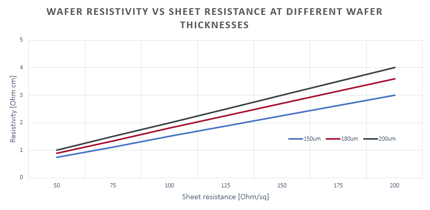
PV-wafers come as mono and polycrystalline with p and n type doping. The sheet resistance depends on the wafer thickness and the resulting resistivity depending on doping type and doping concentration. The resistivity of wafers varies depending on its manufacturing processes and the distribution of dopants within a wafer block or ingot. Overall, there is a strong variation of resistivities across the manufacturing spectrum. The correlation of wafer resistivity and sheet resistance at typical PV wafer thicknesses are shown below.
Sheet Resistance of Metal Panels
Metal panels for WLP / Fan-out applications with titanium and copper films have a sheet resistance of a few mOhm/sq depending on their thicknesses. SURAGUS provides panel monitoring solutions up to 600 mm x 600 mm panel size.
Sheet Resistance of Metal Sheets
Metal sheets consist of aluminum, brass, copper, steel, tin, nickel and titanium. Very few decorative sheets consist of silver or gold. There are catalyst sheets consisting of e.g. platinum. Most common materials are stainless steel, e.g. 304, and aluminum, e.g. 1100-H14, 3003-H14, 5052-H32, and 6061-T6. Sheets are available in various grades and thicknesses. The sheet resistances are typically within a range of 50 µOhm/sq to 5 mOhm/sq depending of conductivity or resistivity of the material and its thickness. The sheet resistance for specific sheets can be calculated with the SURAGUS sheet resistance calculator.
The temperature of metal sheets significantly affects its resistivity. Therefore inline sheet resistance measurements are used to measure the temperature of e.g. Aluminum sheets in a range for 100 to 500 degree Celsius where optical temperature measurements are challenging. The correlation of sheet temperature and sheet resistance is reliable.
Sheet Resistance of Metal Films
Metal film thicknesses start from one atom layer ranging to micrometer and even millimeter range. Sheet resistances range typically from 1 mOhm/sq for thick layers up to 100 Ohm/sq for thin metal films. Low conductive alloy films such as Tantal-Silicon-Nitride may have a sheet resistance of up to 1 kOhm/sq. The sheet resistance can be calculated with the SURAGUS sheet resistance calculator.
Sheet Resistance of TCOs
TCO (Transparent Conductive Oxide) mainly refers to oxides and composite oxides of metal elements such as In, Sb, Zn, Cd etc. TCO materials are widely used in solar cells, display industry, smart glass and photoelectronic devices. The sheet resistance of TCO materials is rather low and their transparency is high. Popular TCO materials, such as ITO (Indium Tin Oxide), AZO (Aluminum Zinc Oxide) thin films, are deeply investigated and applied in various industries due to favorable optical and electrical properties.
Sheet resistance of TCO normally ranges from 5 Ohm/sq up to 500 Ohm/sq depending on the size and its application. In general, doped oxide materials such as ZnO, In2O3, and SiO2 are used for various applications, leading to ITO, IZO, FZO and so on. Dopant concentration and oxidation levels highly influence the sheet resistance of TCO materials. Thin film quality is determined by a number of factors such as thickness, uniformity, surface morphology, optical transparency, and electrical conductivity. For application such as TCM/TCC, it is important to ensure a sheet resistance value as low as possible and an optical transparency as high as possible. In most cases, sheet resistance and transparency have a proportional relation: The lower the sheet resistance, the lower the transparency would be.
Sheet Resistance of Graphene
Graphene as electrode material is very thin and sensitive. Contact testing with 4PP can cause imprints, defects and contaminations. Therefore, non-contact eddy current testing is strongly recommended. Graphene can come as monolayer, bilayer or multilayer material. If there are more than ten layers involved, then it is typically referred to as graphite. Monocrystalline and polycrystalline graphene can have very different mechanical and electrical properties. The electrical properties of graphene can be very different and typically reach from 30 Ohm/sq to 3,000 Ohm/sq depending on flake size, doping, number of layers and defect density (line defects, folds, gaps). Transferred graphene layers on non-conductive substrates such as PET, Quartz wafers or glass can be characterized with high accuracy in a huge measurement range across the samples.
Sheet Resistance of Nanowire Materials
Please refer to our electrical anisotropy section.
Sheet Resistance Measurement Standards
Several industries apply their own measurements standards for sheet resistance measurement using eddy currents devices. Examples are
- SEMI MF673 — Test Method for Measuring Resistivity of Semiconductor Wafers or Sheet Resistance of Semiconductor Films with a Noncontact Eddy-Current Gauge
- SEMI PV28 — Test Method for Measuring Resistivity or Sheet Resistance with a Single-Sided Noncontact Eddy-Current Gauge
- ASTM F1844 - 97(2016) — Standard Practice for Measuring Sheet Resistance of Thin Film Conductors For Flat Panel Display Manufacturing Using a Noncontact Eddy Current Gage
Testing Devices for Sheet Resistance Measurements
Industry and R&D laboratories have different requirements according to number of measurement samples per day, measurement point density and automation level. In result, four key testing types are commonly applied
- Handheld
- Laboratory / Benchtop
- Single point
- Imaging
- Inline / Tool integrated
- Inline static single / multi-sensor
- Inline transversing
- Robot / tool integration