For product requests contact us by using the
- Contact formular,
- Email (sales@suragus.com) or
- Phone (+49 351 32 111 520).
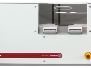
The EddyCus® map 2530 RMT is a bench top scanner particularly suitable for research and technology labs. It is fully functional to measure especially high samples with non-flat surfaces like boules but also for pucks and wafers. It's a compact device, which can measure samples up to 200 mm (8 inch).
 |
 |
 |
 |
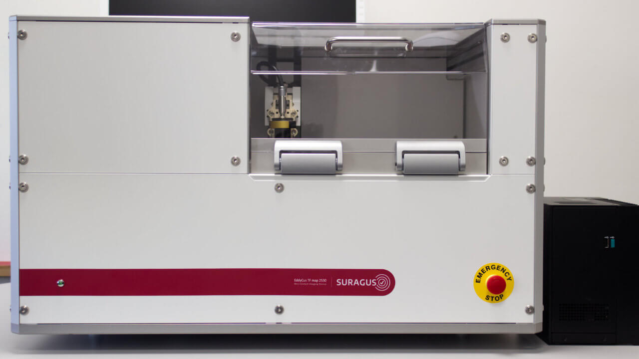
Due to the small spot size of up to only 1 mm of the SURAGUS Sensor XS the EddyCus® map 2530 RMT has a extreme good spatial resolution. Because of that the sensor can measure up to the edge of the sample. That helps to record true measurement values instead of using an extrapolating algorythm to generate an complete image of the sample.
The puck and boule imaging device can measure samples with heights of up to 100 mm and a maximum boule curvature of 10 mm. It can also scan thin samples such as wafers. The device supports sample weights of up to 10 kg, which corresponds to a SiC puck measuring 200 mm in diameter and 100 mm in height. If you need to measure heavier samples, please contact us for more information.


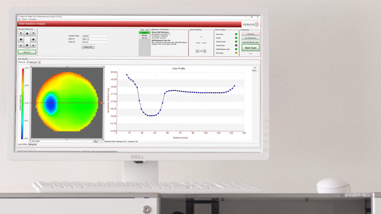
The resolution of a scan depends on the measurement pitch choosen in the recipe and the size of the sample. A boule, puck or wafer with a diameter of 200 mm can have between over 30,000 measurement points (1 mm pitch) to around 300 measurement points (10 mm pitch). The difference in scanning speed is factor 10. The sweet spot between a high resolution and a high speed is the 2.5 mm pitch. Scans with 2.5 mm pitch have around 5,000 real measurement points on a 200 mm boule, puck or wafer.
Due to the high resolution all information remain intact. No interpolation between the measurement points will generate additional information. Therefore a high resolution is crucial for the detection of small defects or imperfections.
To ensure the best possible scanning results, we offer a broad range of sensor types, each with its own strengths and limitations. We carefully analyze each measurement task to determine which sensor is best suited, guaranteeing optimal performance for your specific needs.
For optimal results, it is crucial to position the samples precisely at the center. The inlays are available for samples of various diameters, up to 205 mm. They simplify and accelerate the positioning process, eliminating a potential source of error and ensuring more reliable results.
The EddyCus® map 2530 RMT for boules, pucks and wafers has an easy to use software. After you laid your sample central on the measurement field you
After the scan is finished you can start the analyzing process. You will be able to
For more information please watch our data sheet or contact us by email.
| Measurement technology | High frequency eddy current sensor |
| Substrates | Boules, pucks, wafers |
| Max. scanning area | 8 inch / 205 mm x 205 mm x 100 mm |
| Edge effect correction / exclusion | 2 – 10 mm (depending on size, range, setup and requirements) |
| Max. sample thickness / sensor gap | 100 mm |
| Resistivity range | 0.1 – 100 mOhm·cm (lower and higher on request) |
| Conductivity range | 0.01 – 65 MS/m |
| Pitch | 0.1 – 10 mm |
| Spot size (coil size) Penetration depth (frequency) |
1 – 9 mm (depending on coil size) 1 – 10 mm (depending on frequency) |
| Speed | 150 mm per second (time 1 to 30 minutes) |
| Device dimensions (w/h/d) / weight | 31.5” x 19.1” x 33.5” / 785 mm x 486 mm x 850 mm / 90 kg |
| Further available features | Sheet resistance imaging, metal layer thickness imaging, advanced impedance spectroscopy using EddyEVA |
If you are interested in other solutions you can look at our EddyCus® portable PS or EddyCus® map 2530 RMB.
For product requests contact us by using the