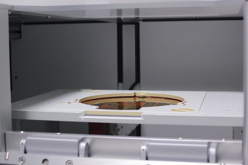
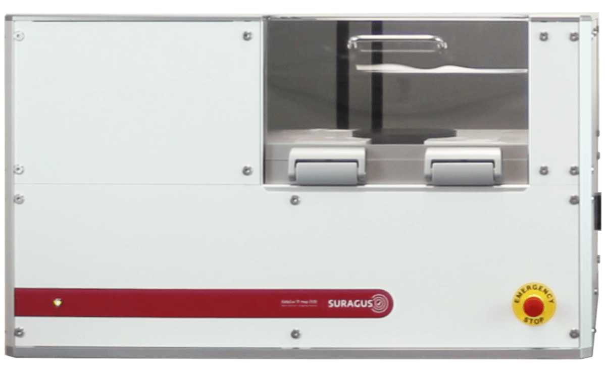
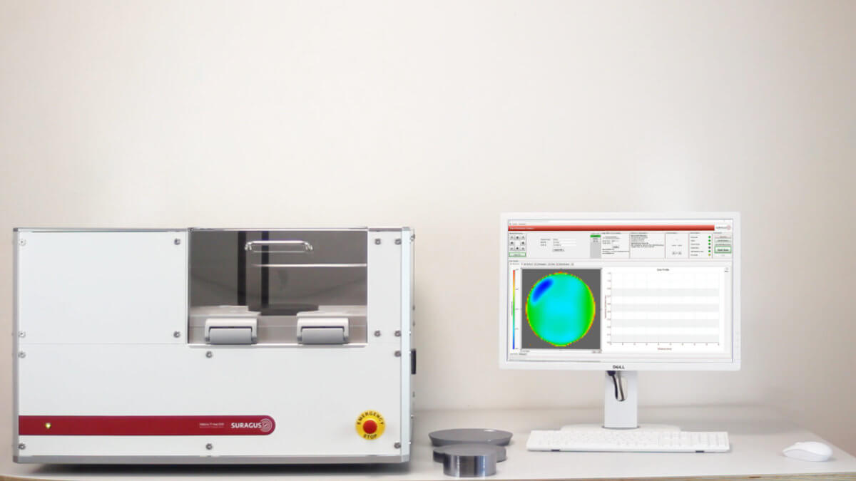
Improved thin-film and substrate quality is achieved through high-resolution mapping enabled by non-contact eddy current technology. The EddyCus® map 2530 RMB, with its minimal spot size, allows for precise measurements in close proximity to the sample edge.
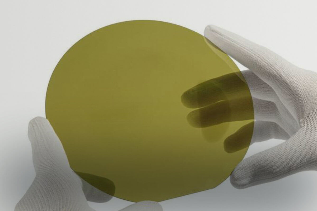
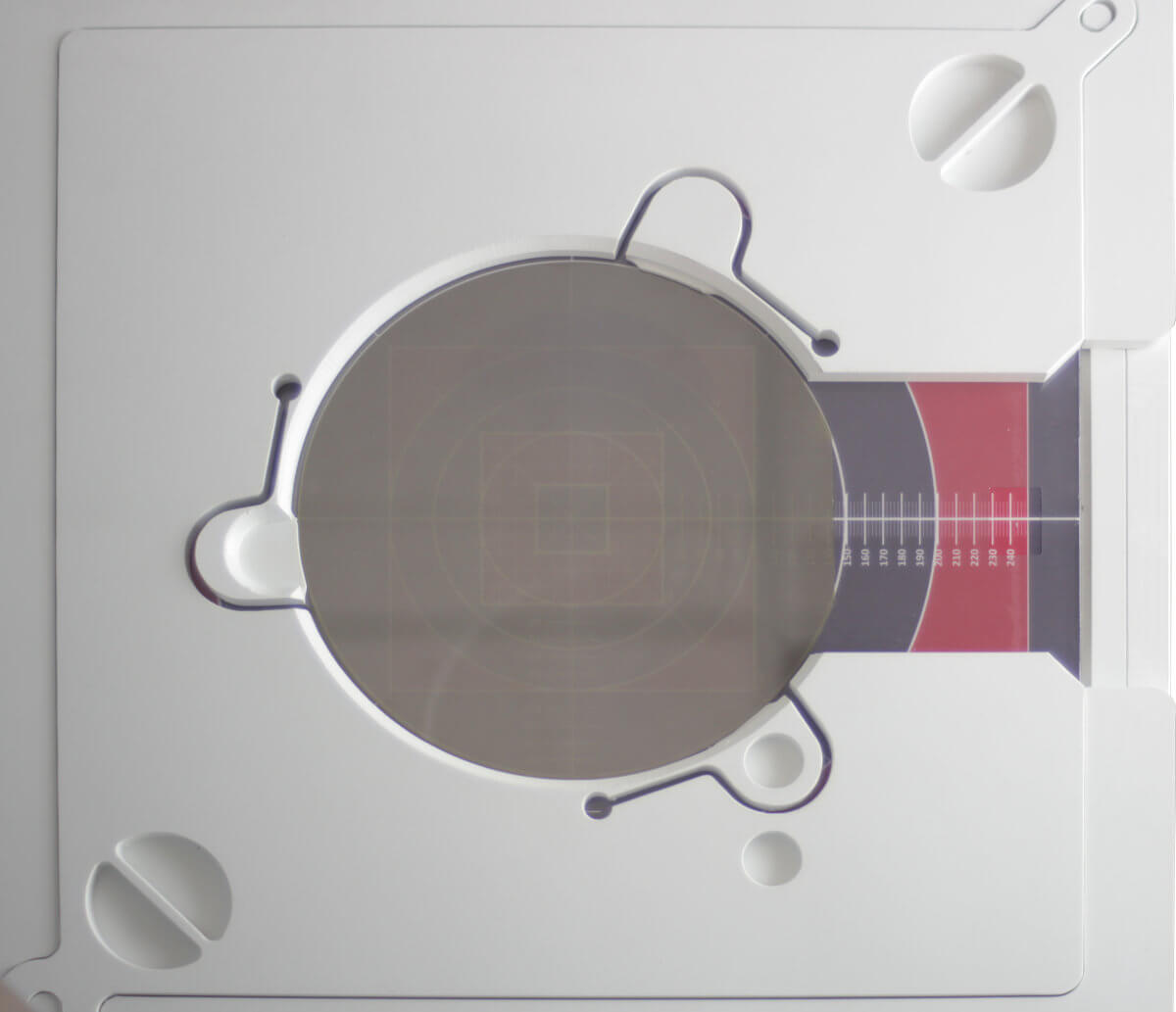
The EddyCus® map 2530 RMB is a non-contact eddy current mapping system specifically optimized for the high-resolution electrical characterization of semiconductor wafers and their metallization layers. Tailored for applications requiring minimal penetration depth, this system is equipped with compact sensors that enable exceptionally small spot sizes—ideal for detailed mapping of thin conductive layers and localized features, including near-edge regions of wafers.
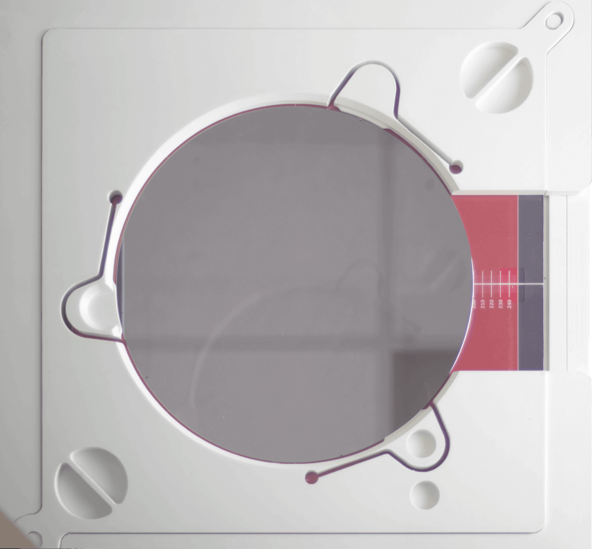
Although optimized for wafers, the system can also accommodate small bulk samples such as boules or pucks with dimensions up to 50 mm in height and 100 g in weight, providing added flexibility for R&D and quality control workflows.
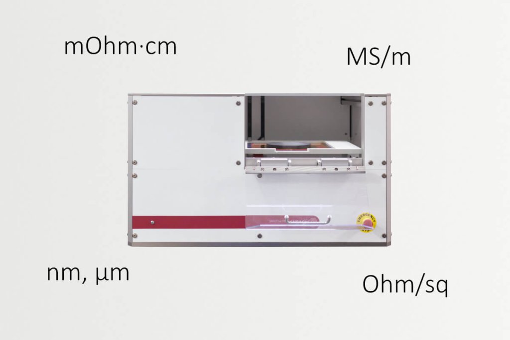
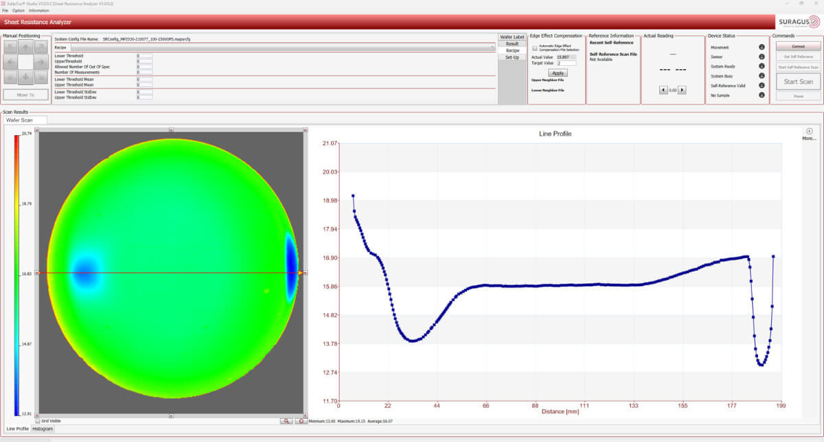
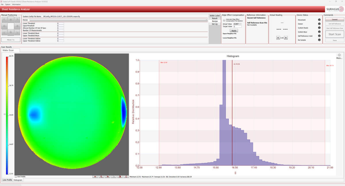
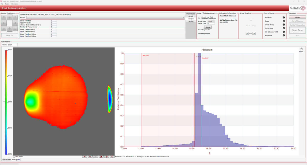
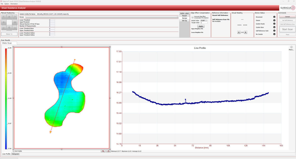
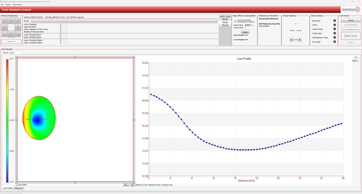
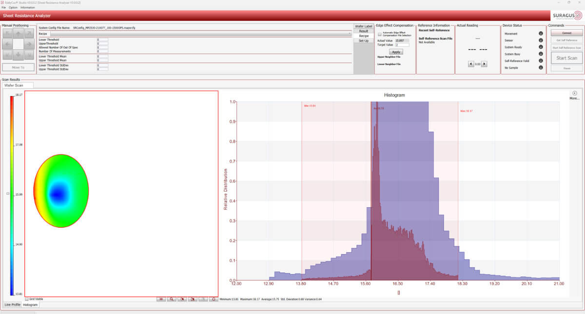
Designed to deliver spatially resolved imaging of key electrical parameters—such as sheet resistance, bulk resistivity, and derived conductivity metrics—the EddyCus® map 2530 RMB enables precise visualization of material homogeneity, dopant distribution, metallization uniformity, and defect structures. It supports advanced eddy current imaging (C-Scan) with a selectable measurement pitch ranging from 100 µm to 10 mm, and is capable of scanning 2D and 2.5D sample areas up to 220 × 220 mm (8 × 8 inches).
The system can be pre-configured from a range of sensor heads to suit different application requirements: high-resolution mapping for thin films and metallization layers, high-penetration probes for bulk analysis.
该设备通常用于
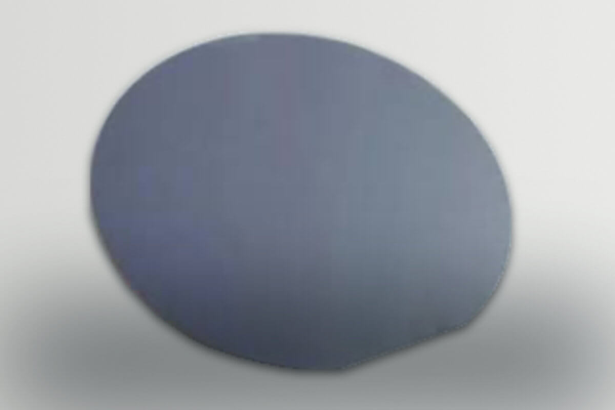
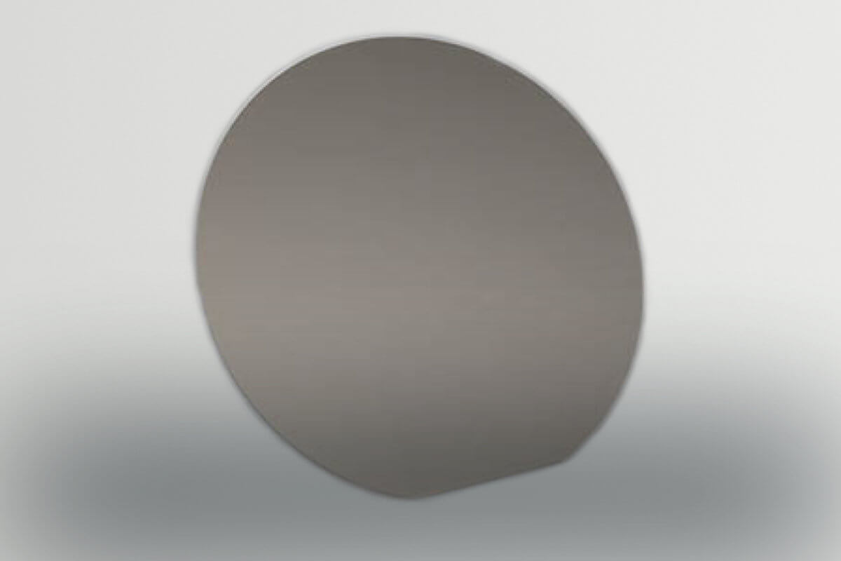
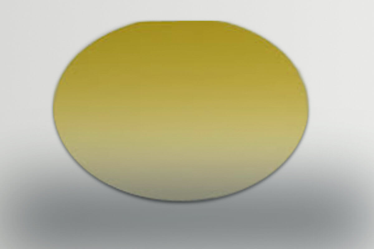
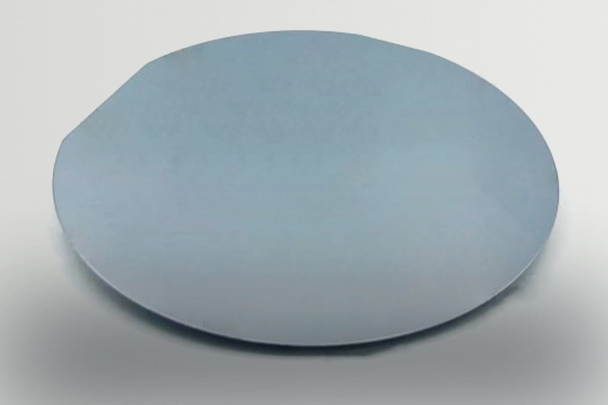
Wafer resistivity imaging
Wafer metallization thickness or sheet resistance imaging
样品尺寸:50 x 50 毫米至 300 x 300 毫米
Various sensors dedicated to specific measurement task