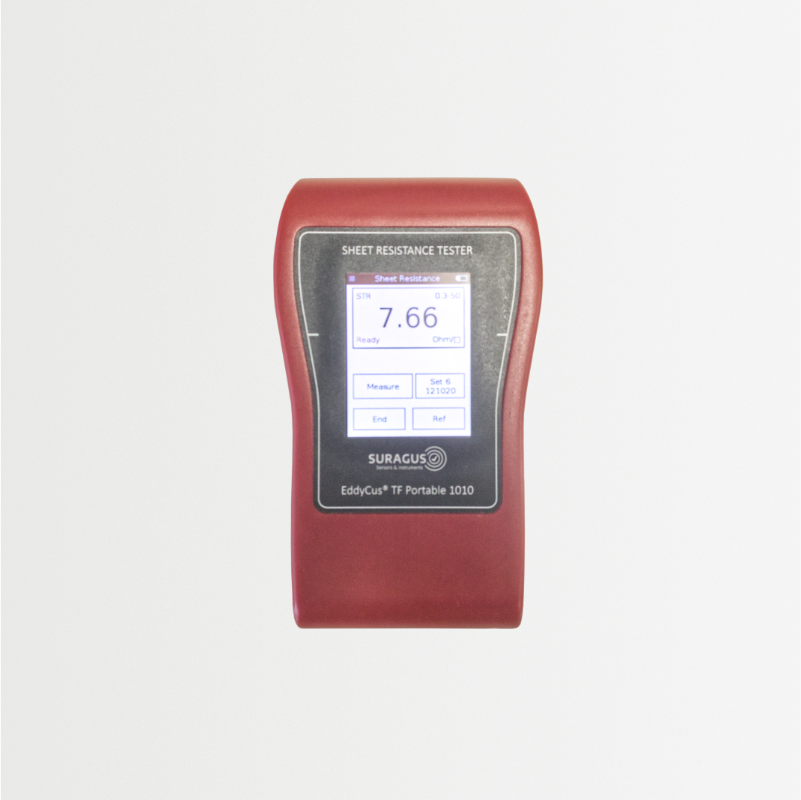
EddyCus® portable Series
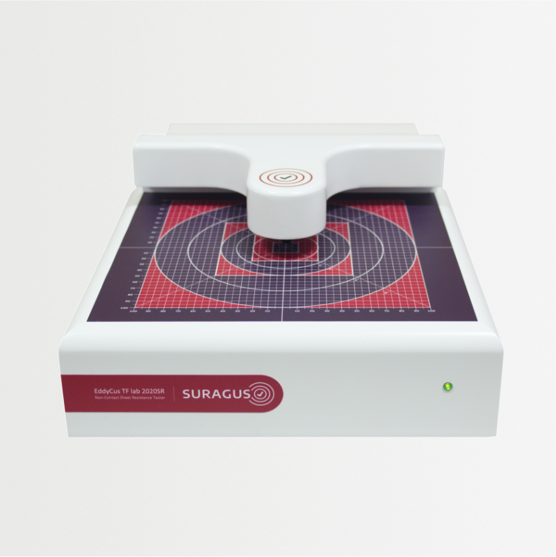
艾迪库斯®实验室系列
埃迪库斯®地图系列
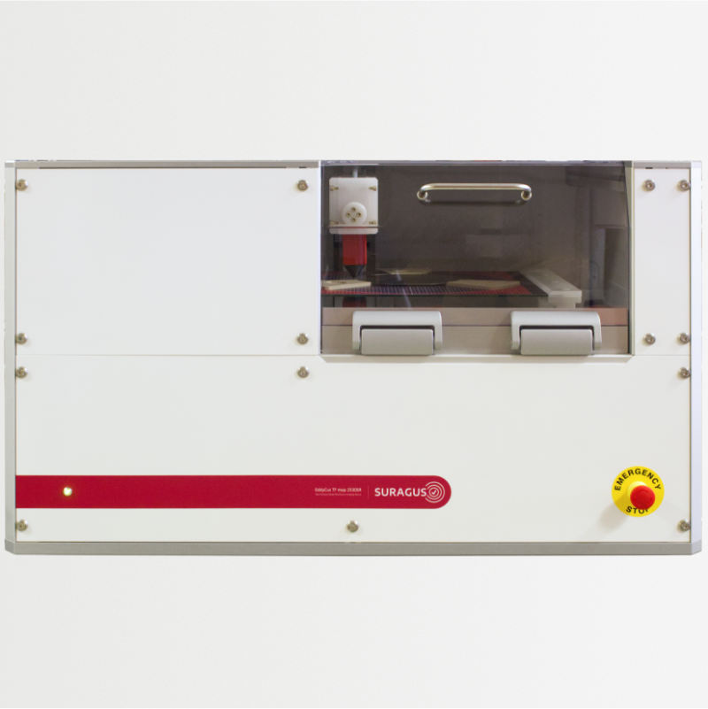
艾迪库斯®直列系列
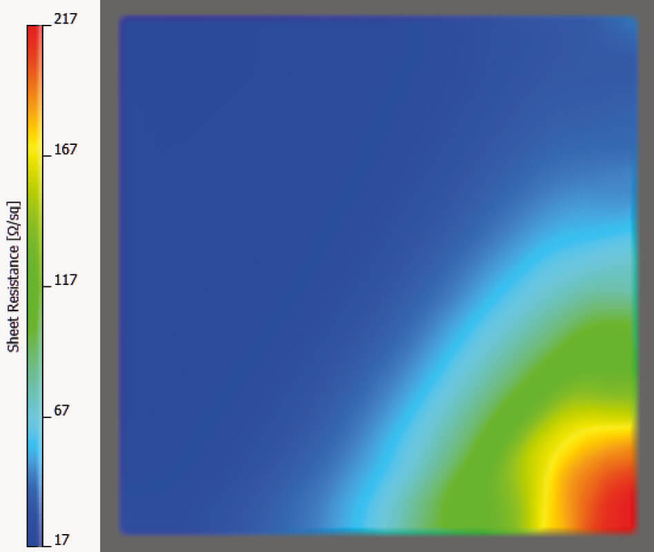
50 x 50 mm metal film withstrong deposition profile
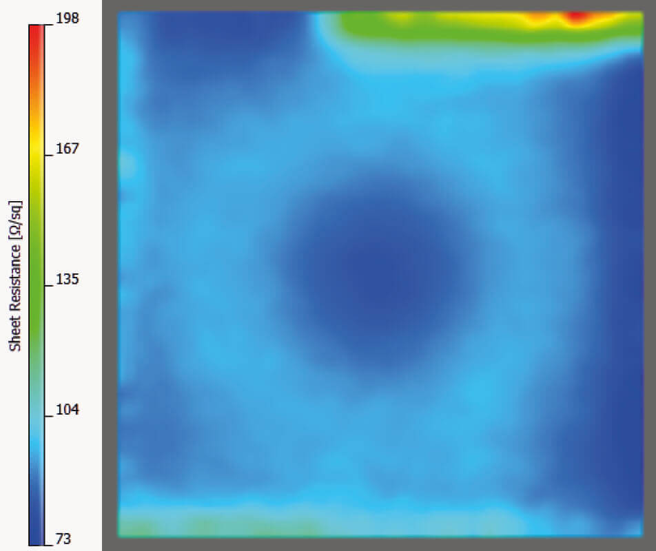
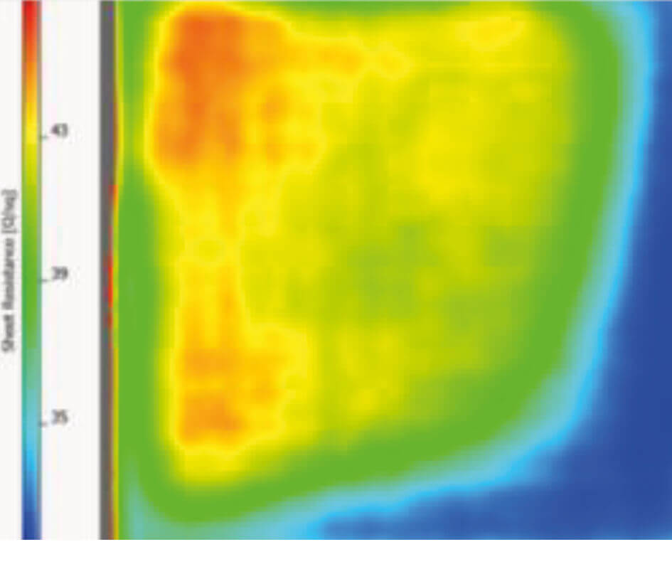
100 x 100 mm AZO withdonut and side effect
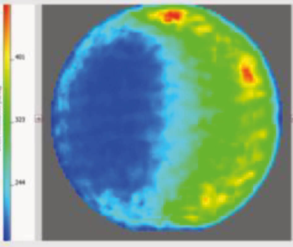
4 inch graphene on quartz waferwith selective doping
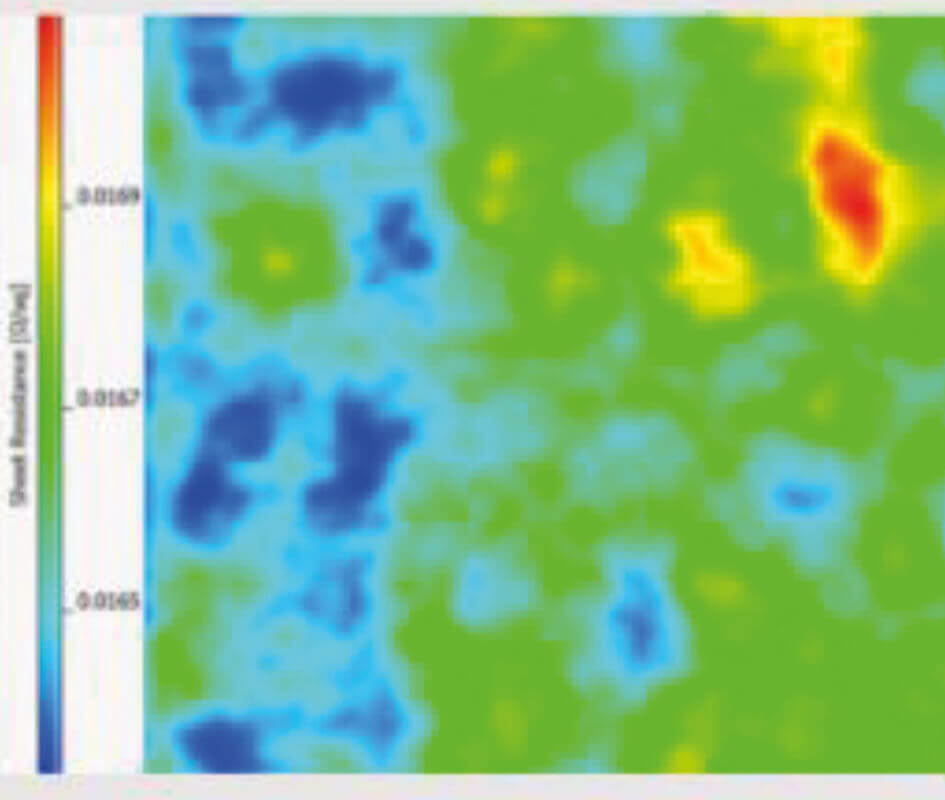
150 x 150 mm Graphite plate
Poly-SI-Solar wafer 156 x 156 with different doping profile