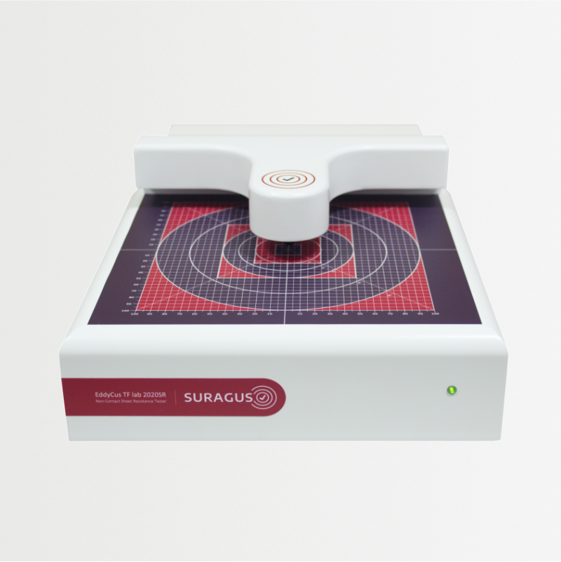
EddyCus® lab Series
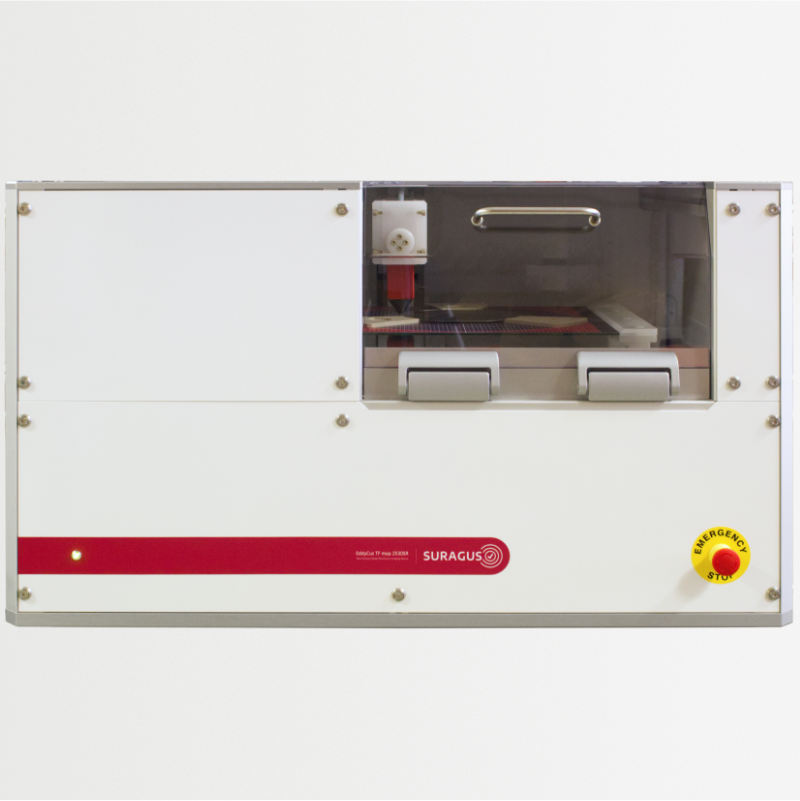
EddyCus® map Series
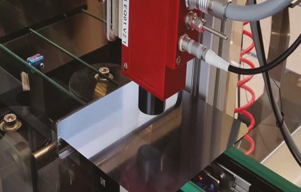
EddyCus® inline Series
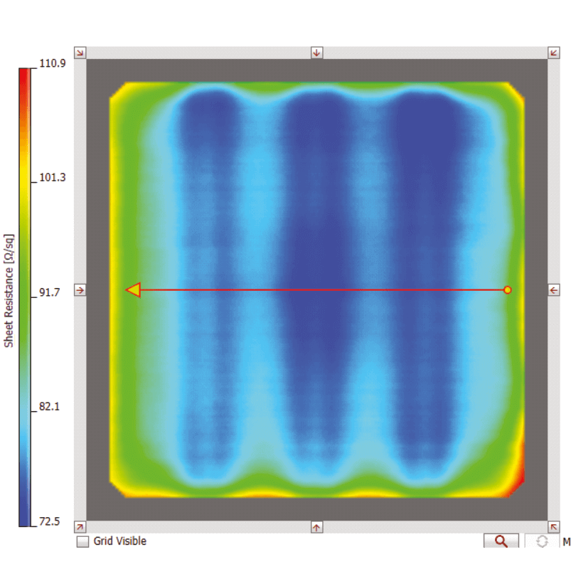
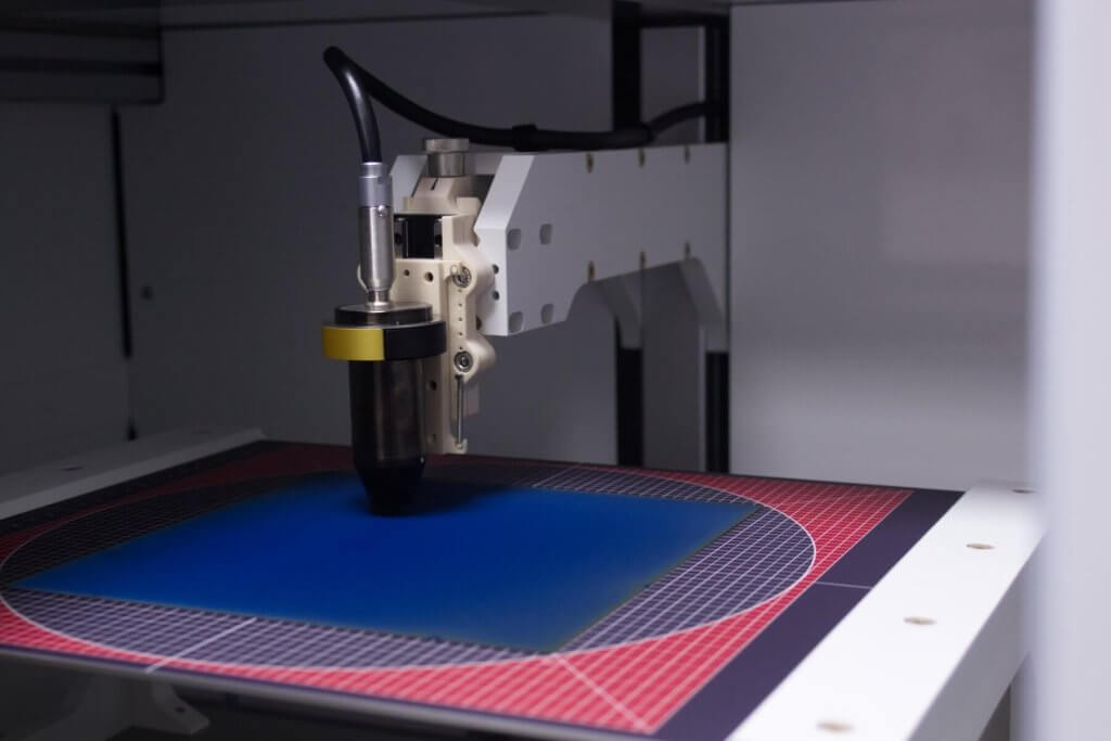
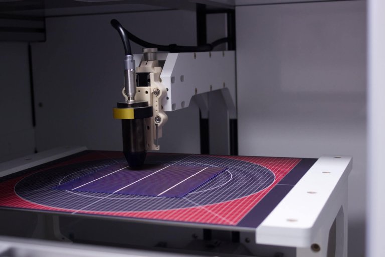
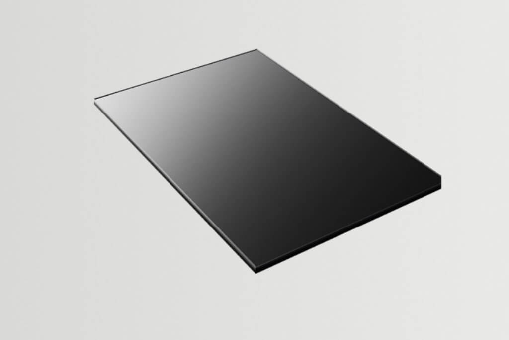
P-doped Monocrystalline Silicon Wafer
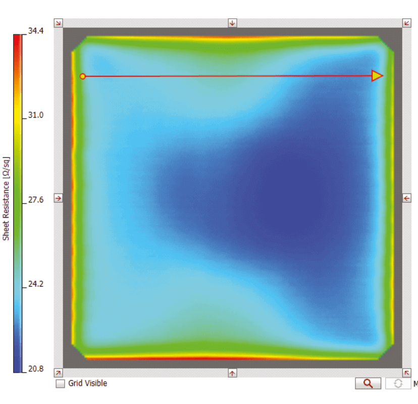
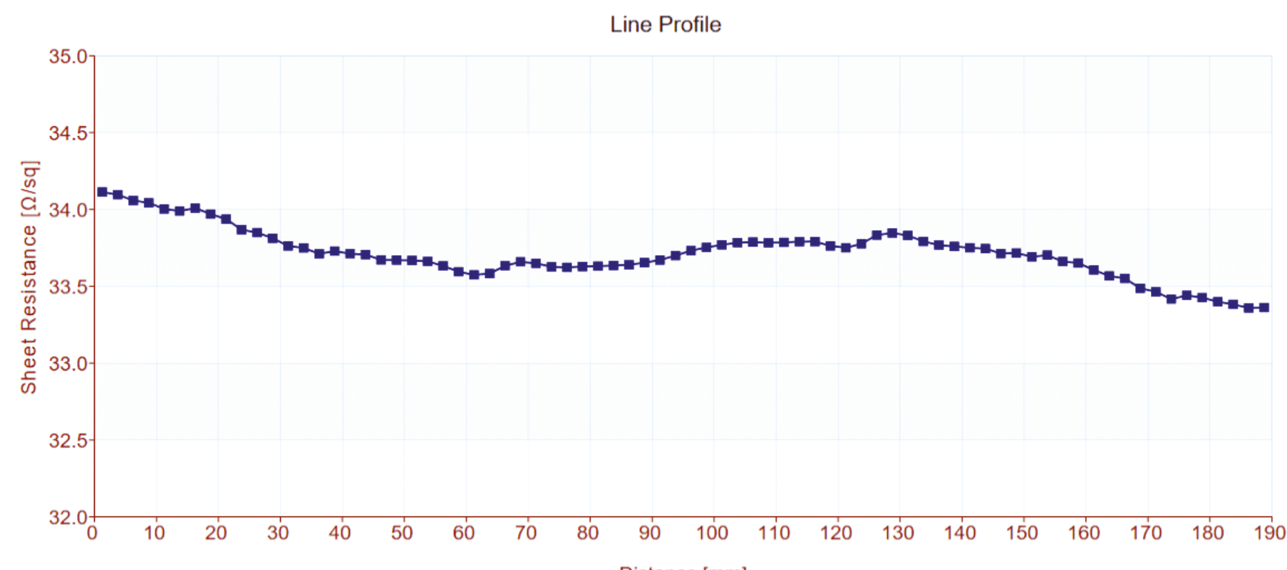
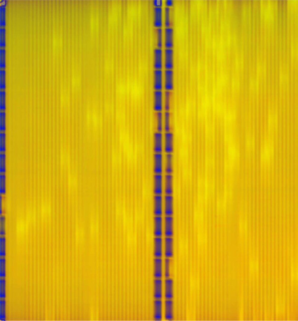
Line Profile Analysis Exposes Homogeneity