For product requests contact us by using the
- Contact formular,
- Email (sales@suragus.com) or
- Phone (+49 351 32 111 520).
The EddyCus® map C2C is a fully automated measurement device for full area characterization of wafer substrates or coatings to ensure process reliability and quality assurance, in the semiconductor industry.
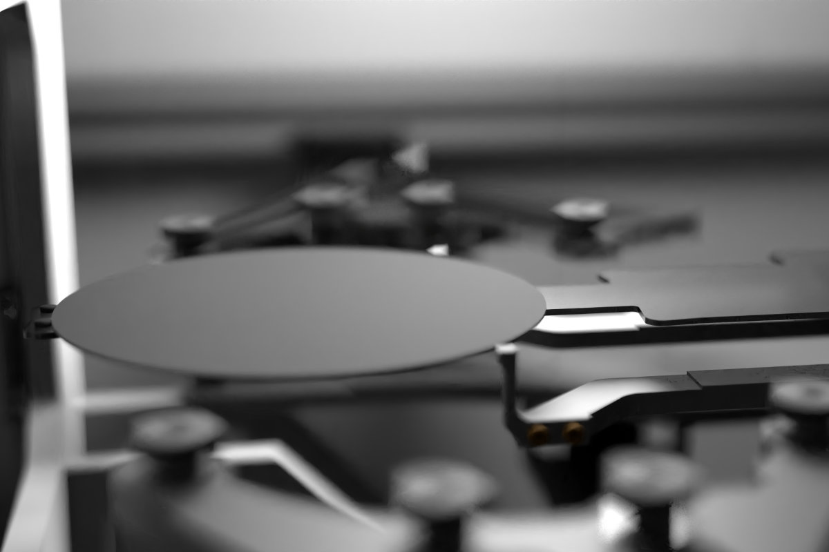
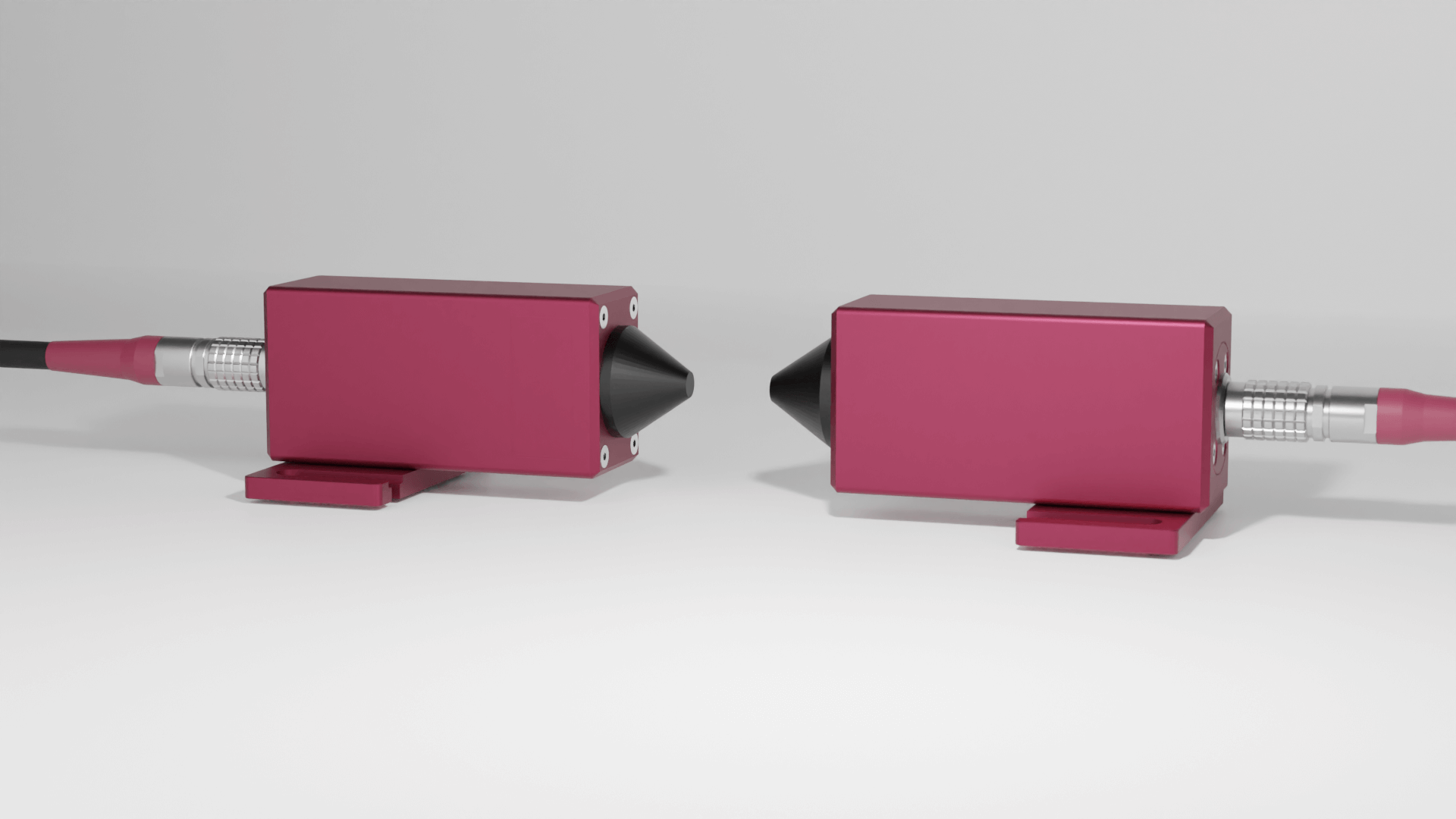
The system is equipped with two non-contact eddy current sensors operating in transmission mode. This allows the homogeneity of the substrate material or conductive coating to be displayed in great detail.
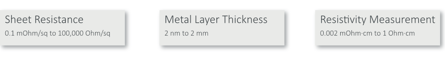
Our system is capable of measuring the sheet resistance or metal film thickness of a thin film as well as the resistivity of the wafer substrate.
During the development of the device, emphasis was placed on reducing contacts of the system with the wafer to a minimum in order not to influence the integrity of the wafer. Therefore, the device works almost completely non-contact. The surface of the wafer substrate or coating is not touched. Contact is only made selectively and with little force on the side surfaces of the wafer. Please have a look at our video of the EddyCus® map C2C to understand the handling process.
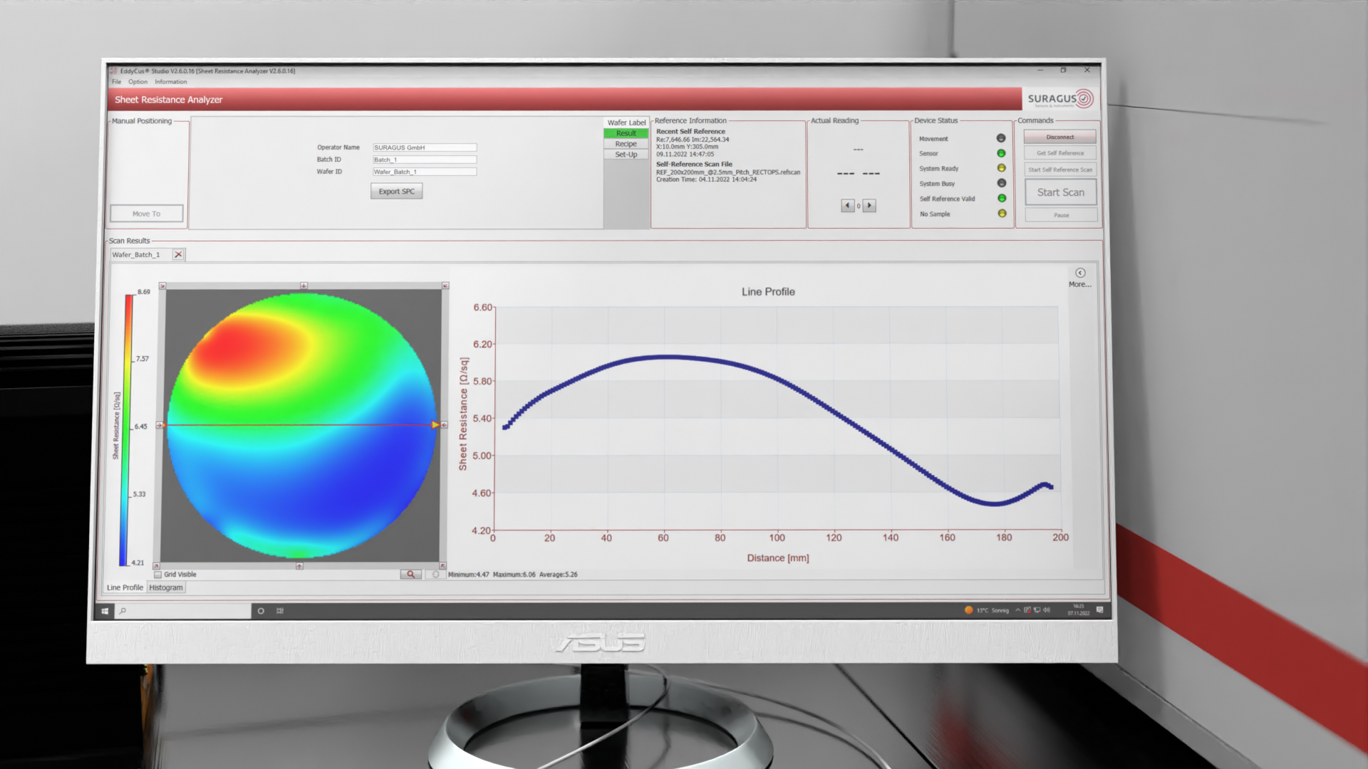
The measuring device creates a high-resolution, full-area imaging of the wafer or coating, which gives you a deep insight into the quality of the characterized wafer. Depending on the setting and your time requirements, imagings with a few dozen to several tens of thousands of measurement points are possible.
The software also offers various analysis tools, such as a histogram or various line profiles. To view an area on the wafer in particular detail, you can select the relevant location with the selection tool and analyze it again using line profiles or the histogram.
The EddyCus® map C2C has a loading device that can hold a wafer carrier with 150 mm (6 inch) wafers and 200 mm (8 inch) wafers. The wafer carrier has a capacity of 25 wafers.
For wafer imaging, the wafer is transferred from the cassette/carrier to the eddy current sensor and then put back into the cassette. A useful tool for manufacturing businesses looking to cut down on the time spent handling wafers is automated wafer handling. Our automated wafer handling technology lowers labor costs, boosts processing accuracy, and lowers the possibility of human error. Wafers are measured, handled, and transported precisely by the system from the cassette to the measuring station and back to the cassette. By doing this, human manipulation of the wafers is no longer necessary, which prevents measurement errors and potential wafer damage.
A type of semiconductor material known as a wide band gap material has an energy bandgap that is broader than that of a typical semiconductor. Transistors and other integrated circuits are made using wide band gap materials in the semiconductor sector. These components are crucial for semiconductors because they provide greater power efficiency and quicker switching times. Wide band gap materials are appropriate for high-power applications because they also have larger breakdown voltages. They are better able to withstand radiation, which makes them perfect for use in space applications. Silicon carbide, gallium nitride, and diamond are a few examples of materials with a wide band gap. Many different applications, such as power supply, solar cells, and laser diodes, utilise these materials.
The EddyCus® map C2C is able to determine the sheet resistance and thickness of a thin film as well as the electrical resistance of a wafer substrate. The device has a large measuring range, which means that almost all conceivable applications can be measured by the device.
For more information please watch our data sheet.
| Measurement technology | Non-contact eddy current sensor, Capacitive or confocal sensor for TTV |
| Substrates | 6 / 8 inch wafer |
| Cassettes | 1 |
| Edge effect correction / exclusion | 2 – 10 mm (depending on size, range, setup and requirements) |
| Sheet resistance range |
0.0001 – 100 Ohm/sq < 1 – 3 % accuracy 100 – 100,000 Ohm/sq < 1 – 5 % accuracy (6 decades with one sensor) |
| Total thickness measurement | 10 – 100,000 μm (optional) |
| Thickness measurement of metal films (e.g. Aluminum, Copper) | 2 nm – 2 mm (in accordance with sheet resistance) |
| Measurement patterns (line scan, mapping) | 2 nm – 2 mm (in accordance with sheet resistance) |
| Thickness measurement of metal films (e.g. Aluminum, Copper) |
Pitch 1 / 2 / 5 / 10 / 20 / 50 mm Points 9 / 17 / 49 / 81 / 99 / 169 / 625 / .... / 10,000 |
| Measurement time | Line scans in less then 1 second Multi point: 0.1 to 1 second per point |
| Safety variants |
System protected by safety laser scanners Closed system |
| Device dimensions (w/d/h) | 785 mm x 1,170 mm x 666 mm / 30.91“ x 46.06“ x 26.22“ |
| Available features | Resistivity, metal thickness, total thickness variation sensor |
For product requests contact us by using the