Non-Contact Process and Quality Monitoring
for Conductive Materials and Coatings
highly flexible inline measurement solutions, seamlessly adaptable to your specific production process.
- Non-contact real time measurement
- High measurement speed up to 1,000 measurements/ sec.
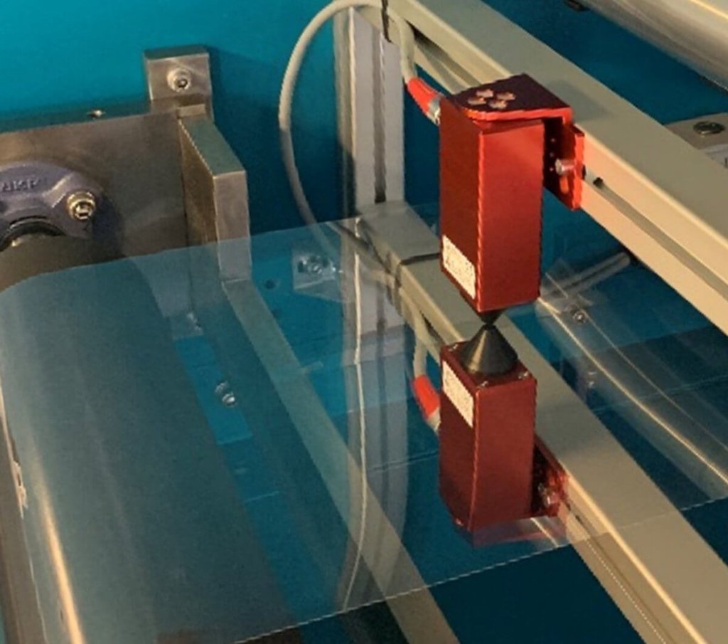
- Fixed sensor installation or traversing sensor installation
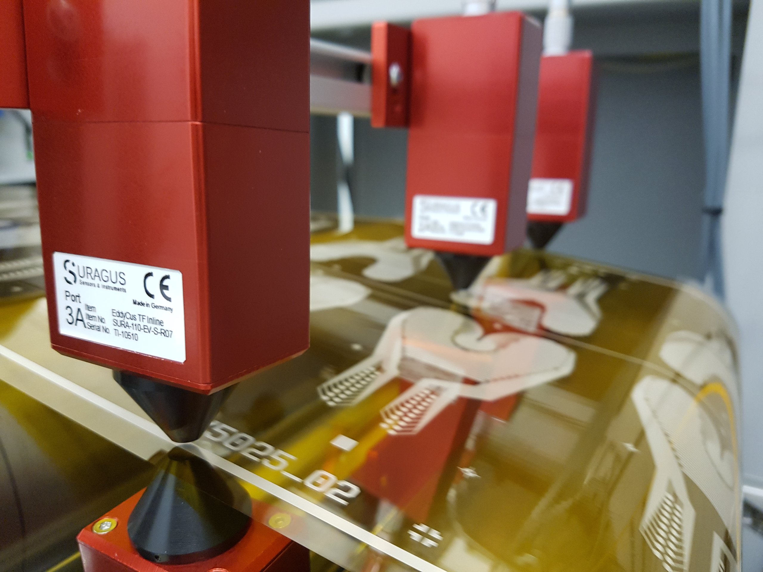
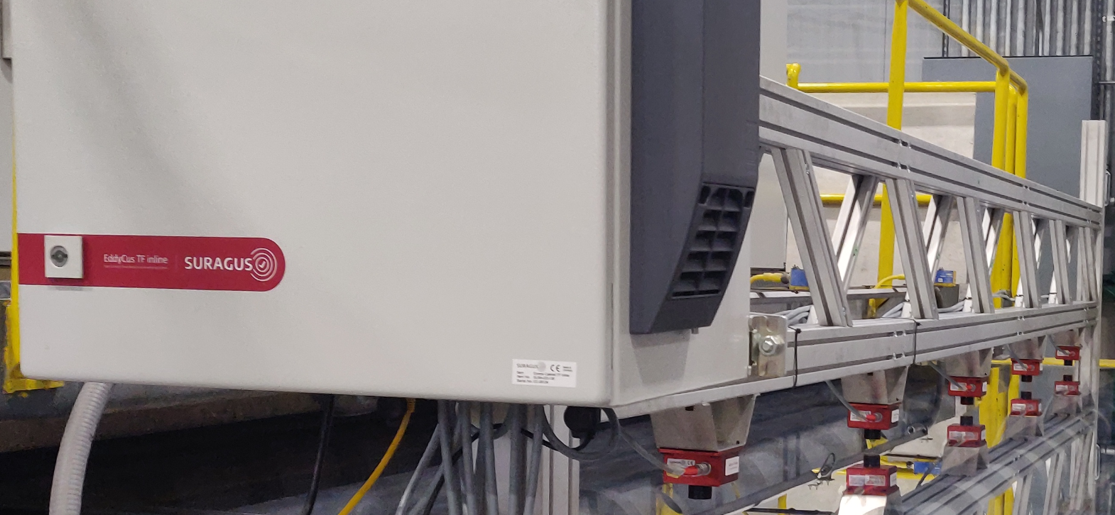
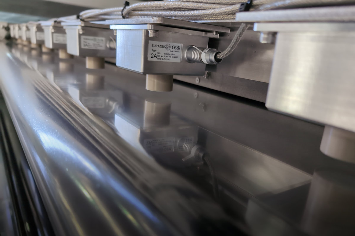
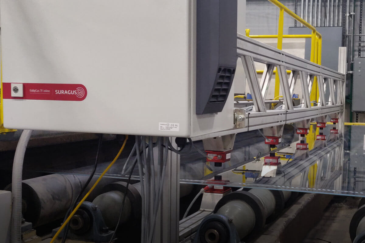
- Integration of 1 – 99 monitoring lanes per system
- Process control at atmosphere or in vacuum
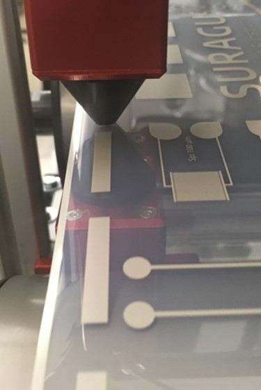
- Measurements very close to the edge of the substrate are possible in many applications
- Long term stability by temperature compensated measurements in changing environment
- Large distances to the testing material (e.g. gap of 60 mm / 2.4 inch)
- Characterization of covered conductive layers or encapsulated substrates
- Numerous software integrated analysis and statistic functions
- Easy set up by EddyCus® RampUp software incl. wizard for system calibration
- Wear- free
Introduction
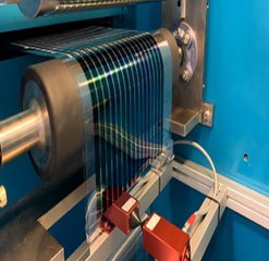
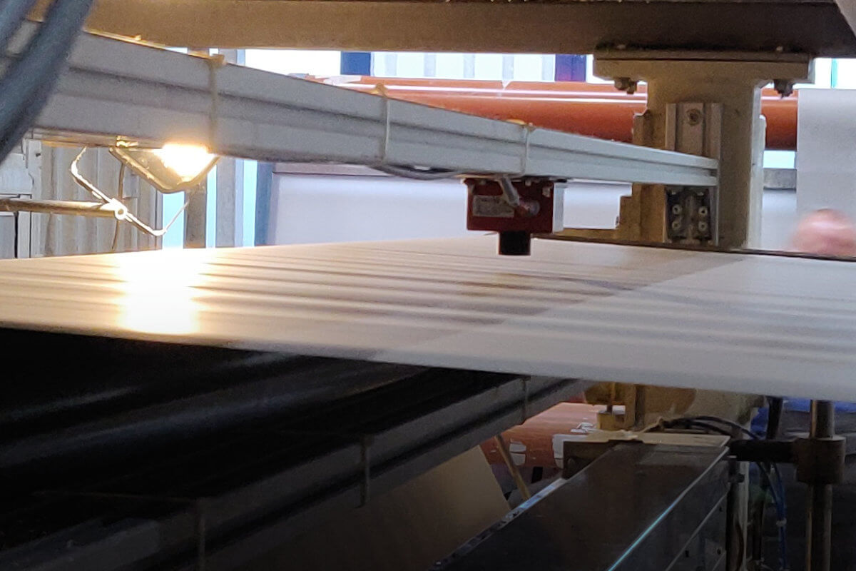
The EddyCus® inline series measures layer properties such as metal layer thickness, sheet resistance, emissivity, residual moisture or grammage in non-contact on various substrates. Relevant substrates are glass, foil, paper, wafer, plastic or ceramic. Monitoring is done by permanent measurement or by trigger events to obtain equidistant results in fast moving coating processes. Monitoring solutions can be implemented either in atmosphere or vacuum conditions. Processes using eddy current technology benefit from high samples rates. Measurement results can be provided for process control systems using customer´s software. Additionally SURAGUS offers the monitoring software EddyCus® EC Control that visualizes, stores and analyses metrology data.
The device is typically used for:
- Process control and quality assurance
- Process time optimization
- Machine utilization
- Material usage
- Productivity
- Product performance improvement (e.g. high transparency and low resistivity, good emissivity, good barrier properties)
- Layer homogeneity especially across large substrates widths
- Predictive maintenance
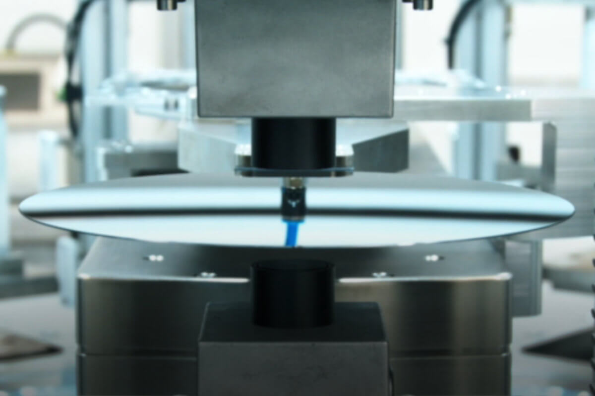
Sensor Capabilities
- Sheet resistance: 0.05 mOhm/sq up to 200,000 Ohm/sq
- Metal thickness: 2 nm – 2 mm (depending material conductivity)
- Resistivity: 0.1 mOhm cm – 1 ohm cm
- Residual moisture (measurement in wet layers by non-contact permittivity measurement)
- Electrical anisotropy: 0.33 to 3 (higher on request)
- Grammage: 0.1 to 1,000 g/sqm
- Emissivity: 0.005 to 0.2
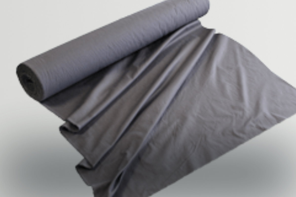
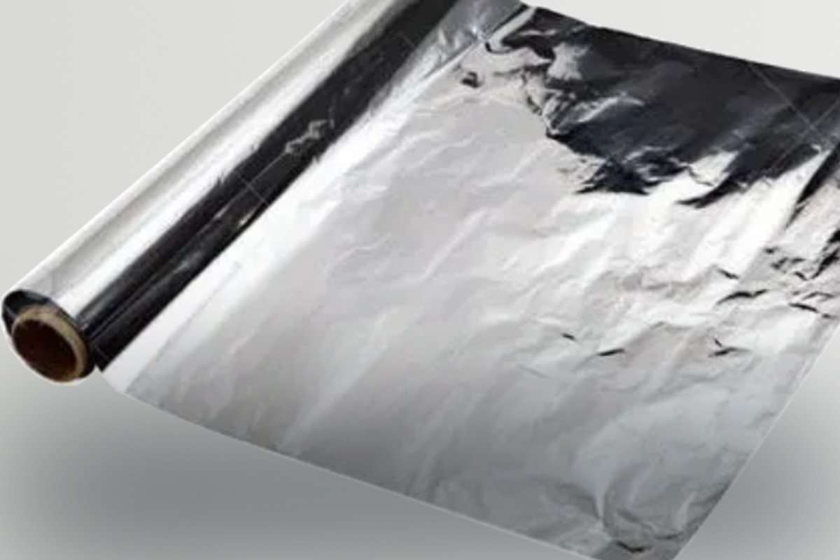
Supported Substrates
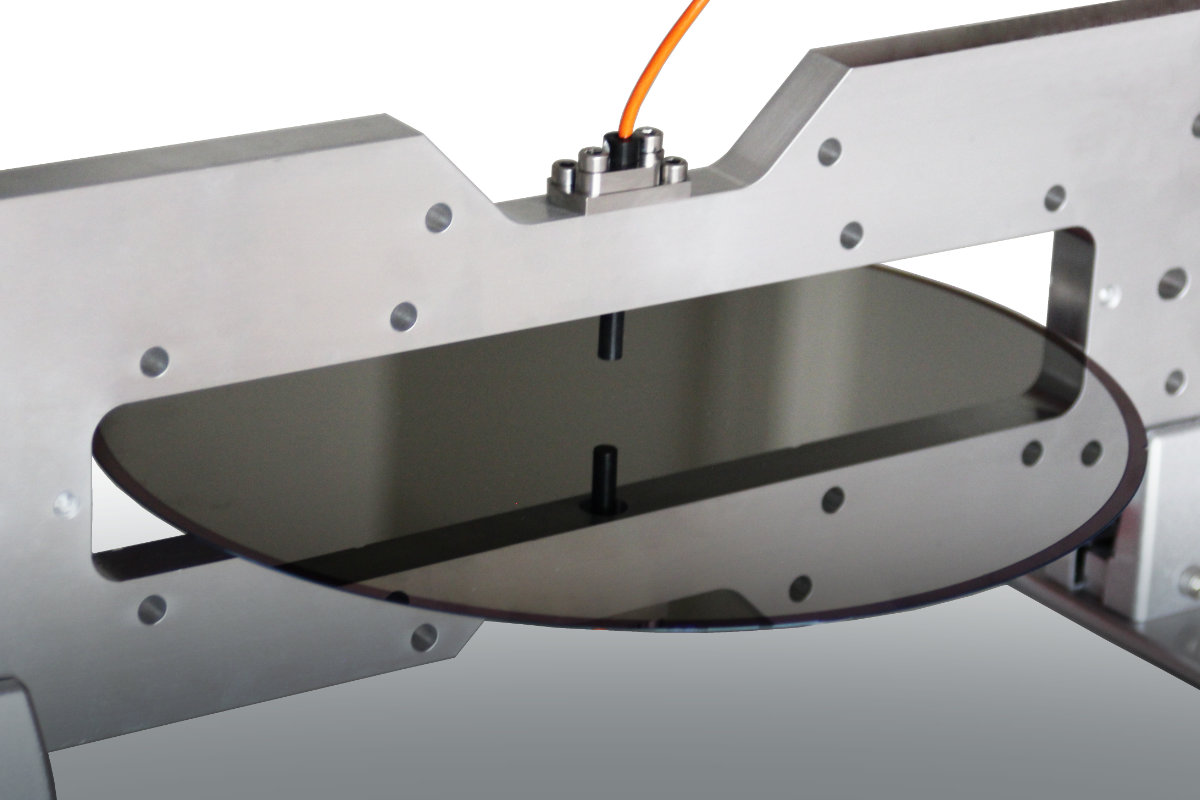
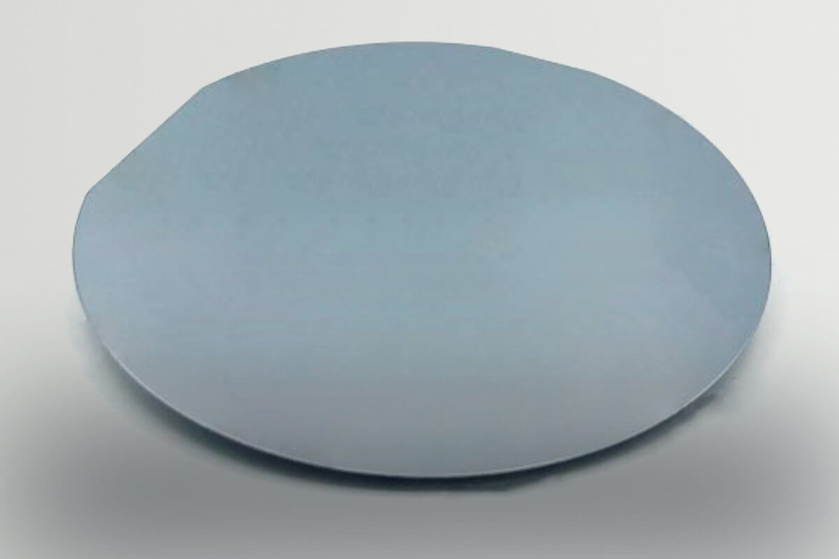
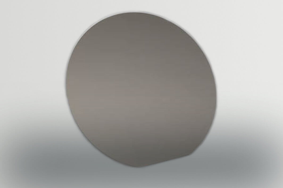
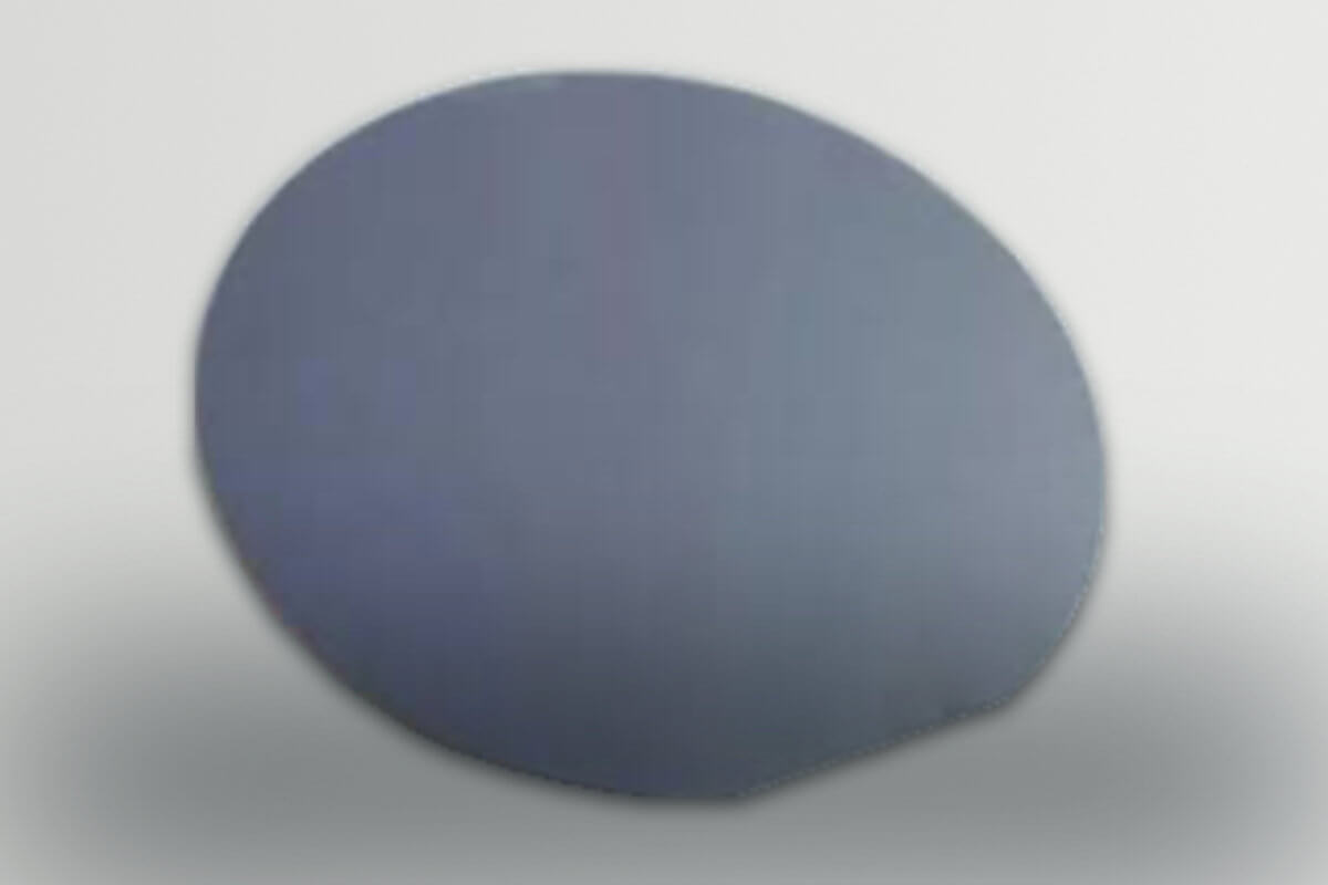
Boules, ingots, pucks, wafer, foils, glass, etc.
Measurement Gap
The gap between both sensors can be
3 / 5 / 10 / 15 / 25 / 50 mm (other upon request)
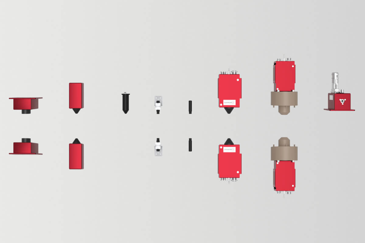
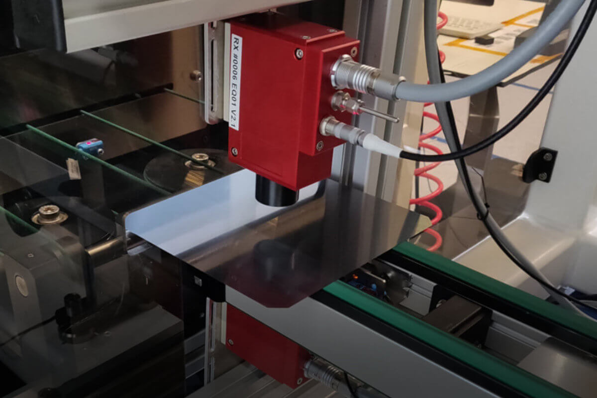
Various Integration Options
To meet your space requirements, SURAGUS offers
- Top mountings or side mountings in combination with
- Different sensor sizes
General Solution
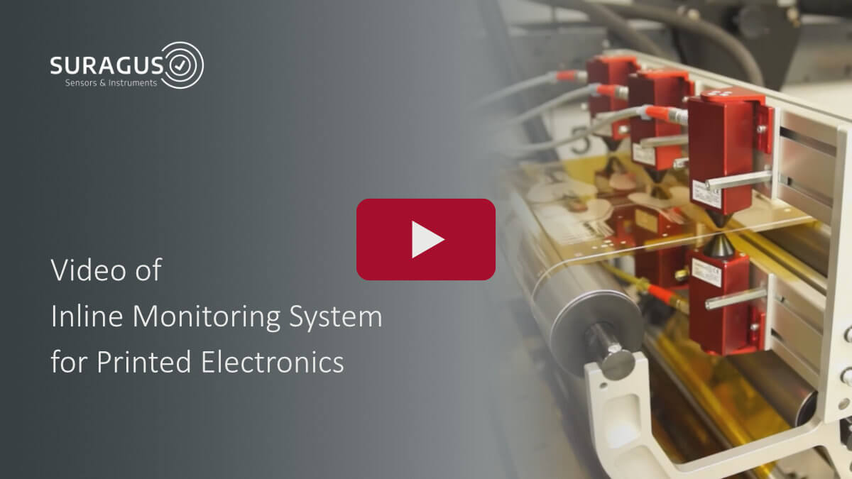
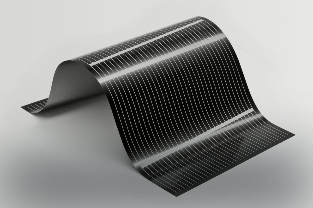
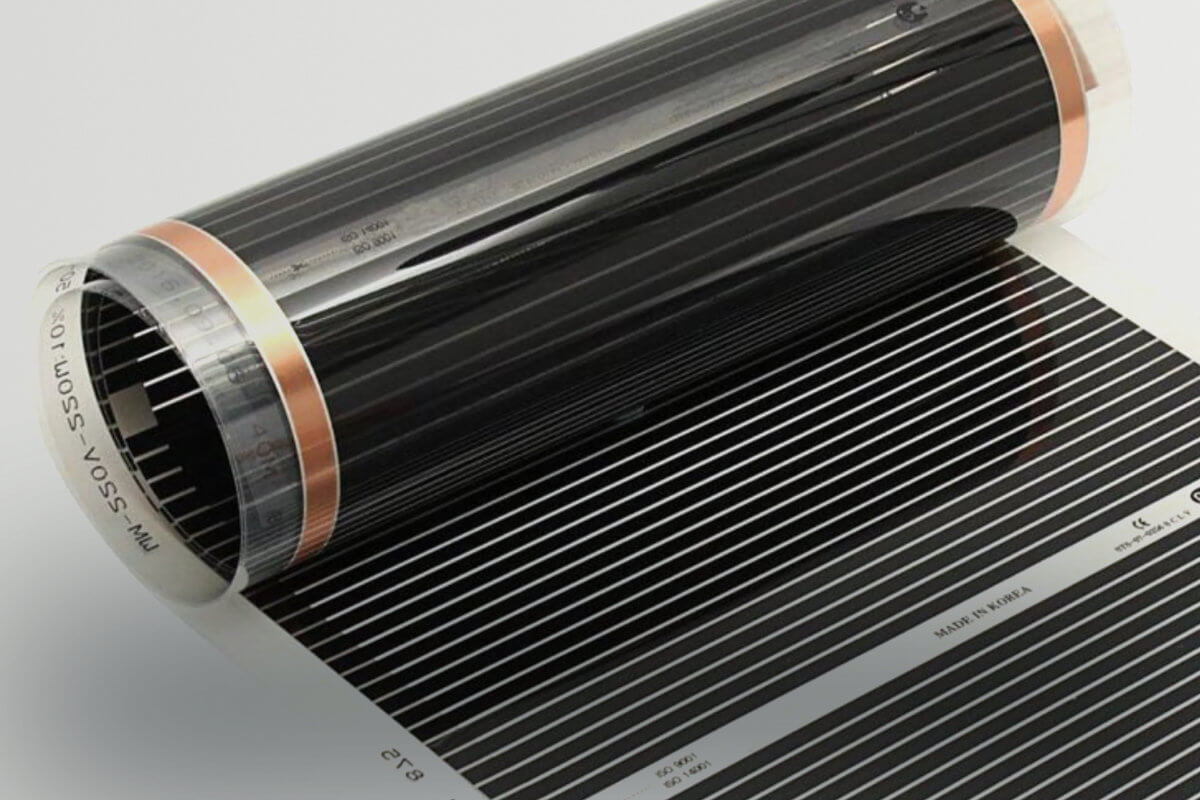
Printed Electronics
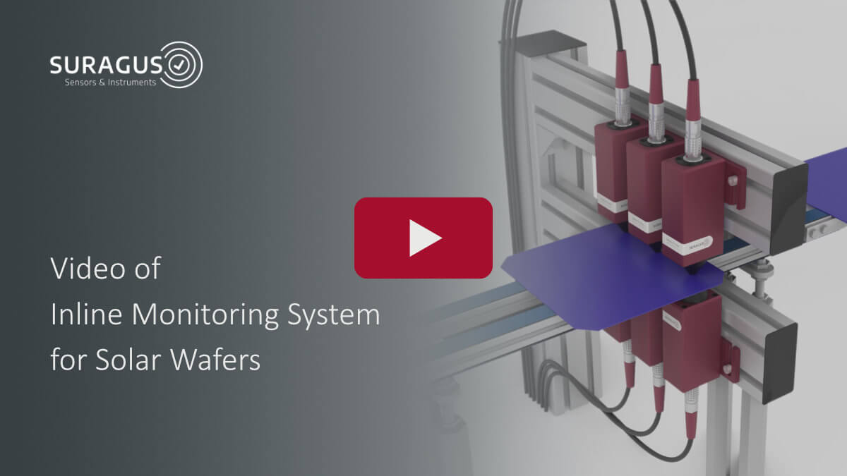
Solar Wafers
Features and Benefits
World Wide Support
High Gap
Fast Database
Instant Results
Continuous Mode with Long Term Stability
Easy to Use Software
Highly Flexible Integration
Since the conditions and requirements in every production facility vary, we have designed sensors in a broad range of sizes and mounting configurations to ensure the optimal solution for any setup.
- Multiple sensor sizes available to match diverse application needs
- Versatile software options
- Standalone software
- Software Development Kit (SDK) for seamless integration
- Data interfaces: Wide range of data interface options for easy system integration
- Suitable for use in a variety of environments
- Features that support flexibility, such as a large measurement gap
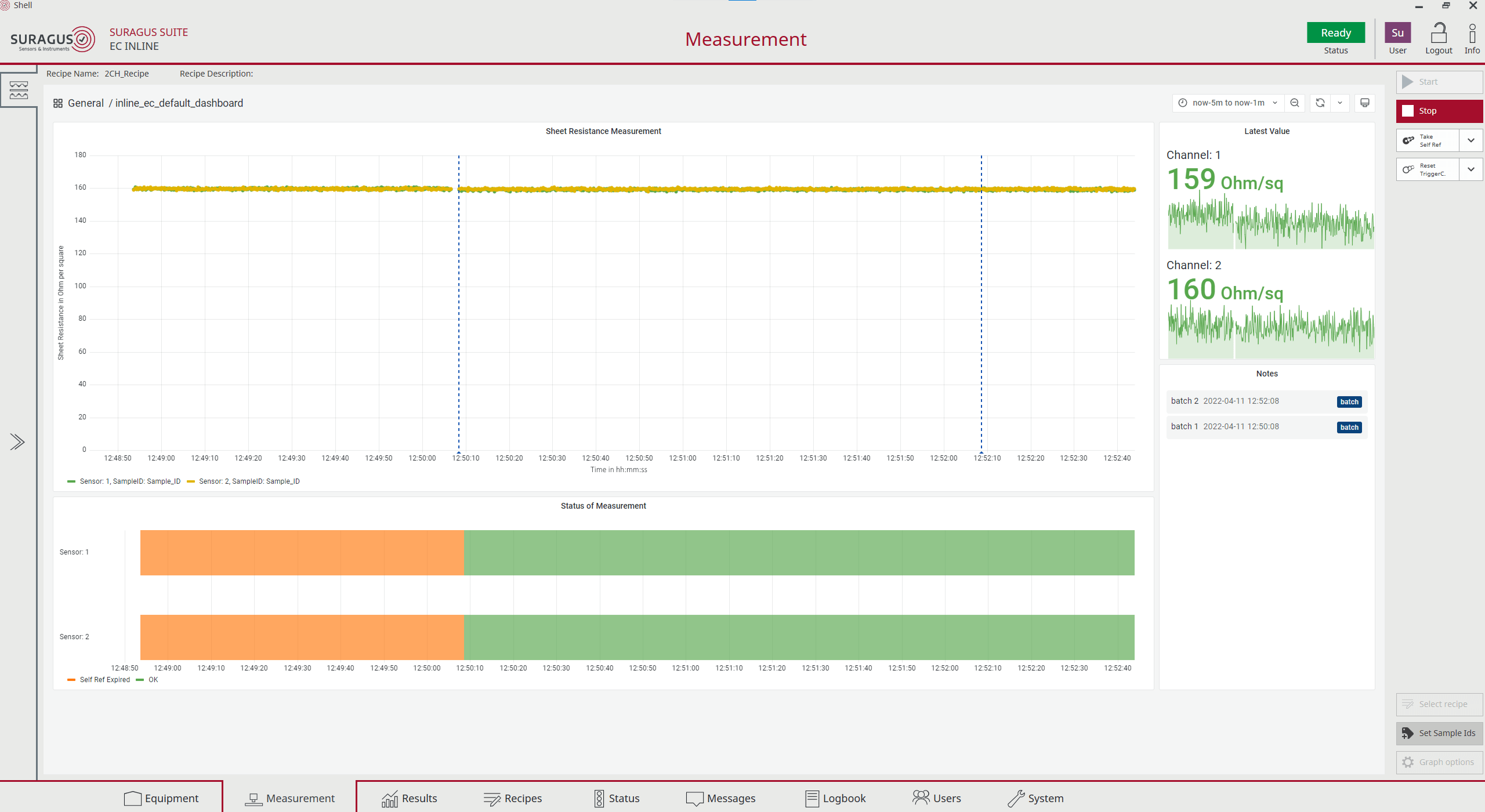
EC inline Control Software
- Graphical live view (different time windows, from 1 minute to 24h)
- Analysis view (data selection from database, statistics)
- Sorting by time, distance, roll number, barcode or Data Matrix code.
- Mode for extending and adapting the calibration
- Parameterization dialog of I/O modules for analog and digital data transmission as well as the parameterization of alarms in case of over/underrun of threshold values
- Automatic and manual data export (csv, txt, xls, …)
- Automatic database cleaning
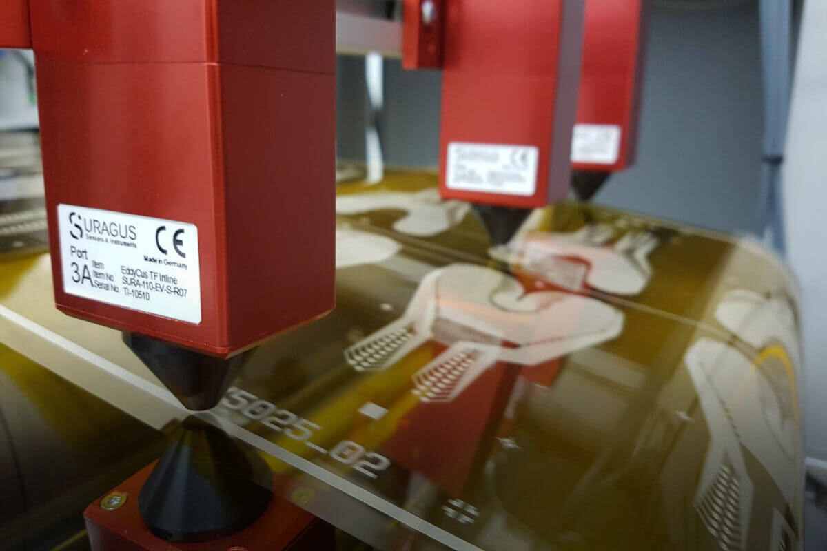
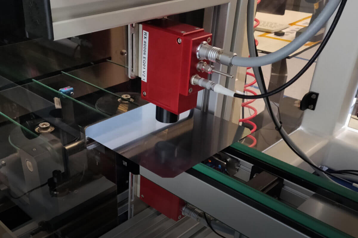
Sensor Form Factors For All Measurement Types
- Sensor S (many options)
- Sensor S – Semi-Vac (vacuum only)
- Sensor M
- Sensor XS
- Sensor XXS
- Customized forms (multi sensors)
Supported Environments
- Atmosphere
- Vacuum
- ATEX
- High temperature version on request
Wiring Setups
- Control cabinet mounting near sensor positions
- Direct mounting tool mounting near sensor positions
- Full sensor integrated hardware
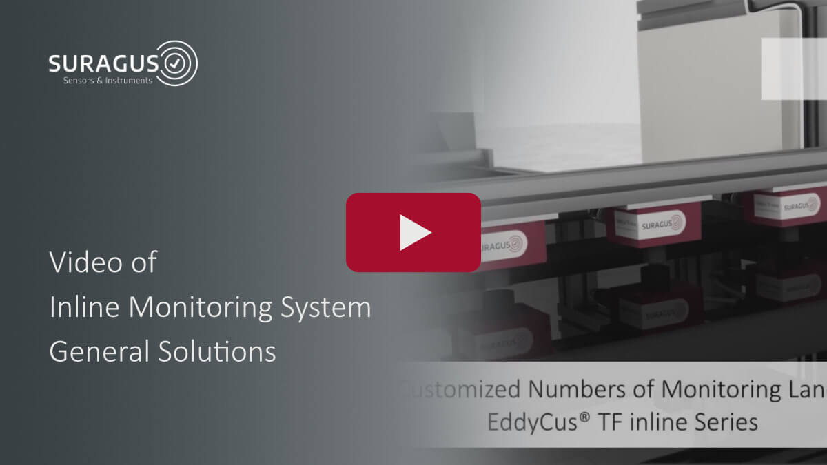
Video of the EddyCus® inline
The video gives you an impression of SURAGUS inline systems.
Inline Solutions
0:16
0:16
Setups Available
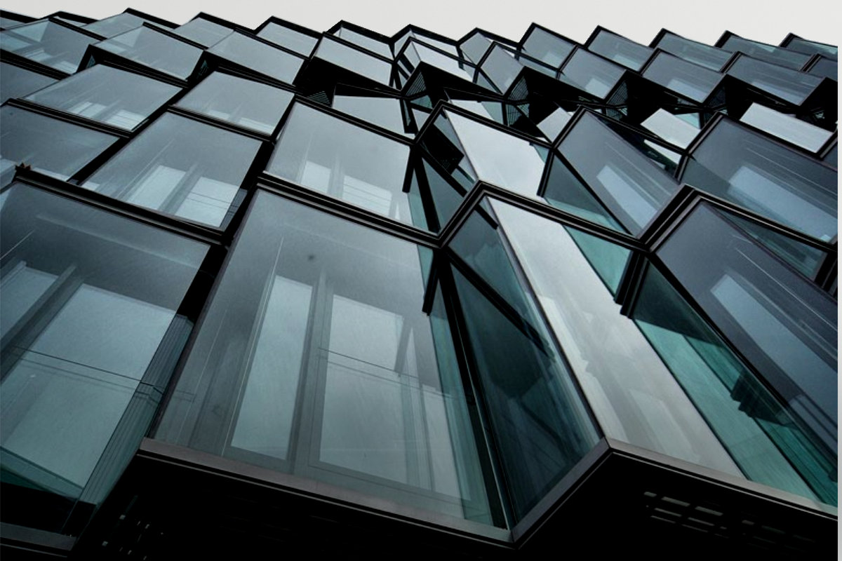
Applications
- Architectural glass (LowE)
- Packaging materials
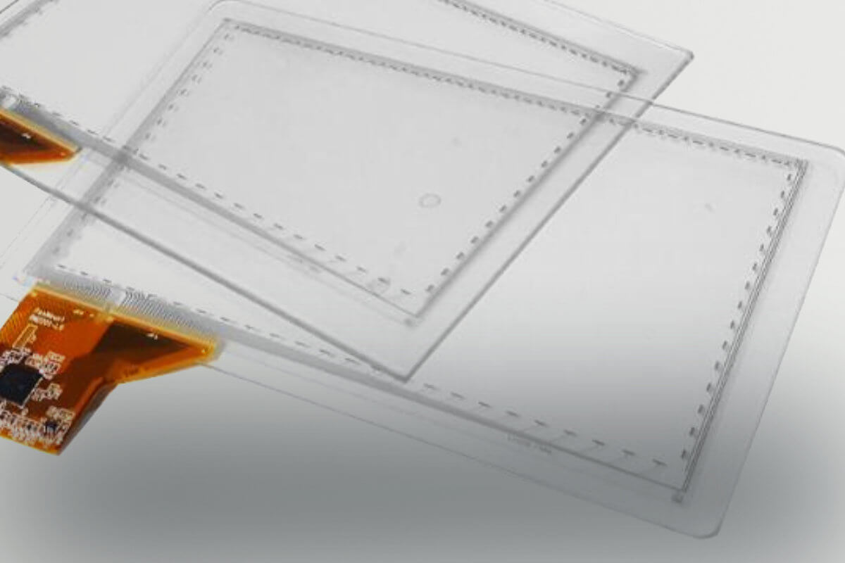
- Displays and touch screens
- Photovoltaics (Thin-film and c-Si)
- Mirror coatings
- Capacitors
- OLEDs and LEDs
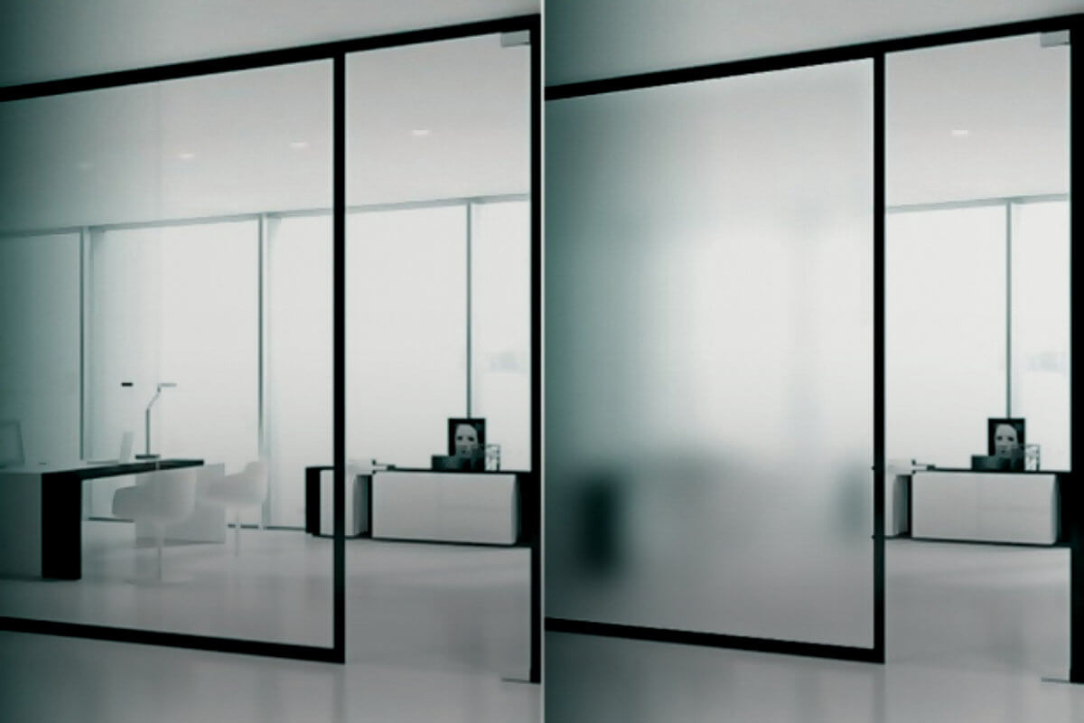
- Smart glass
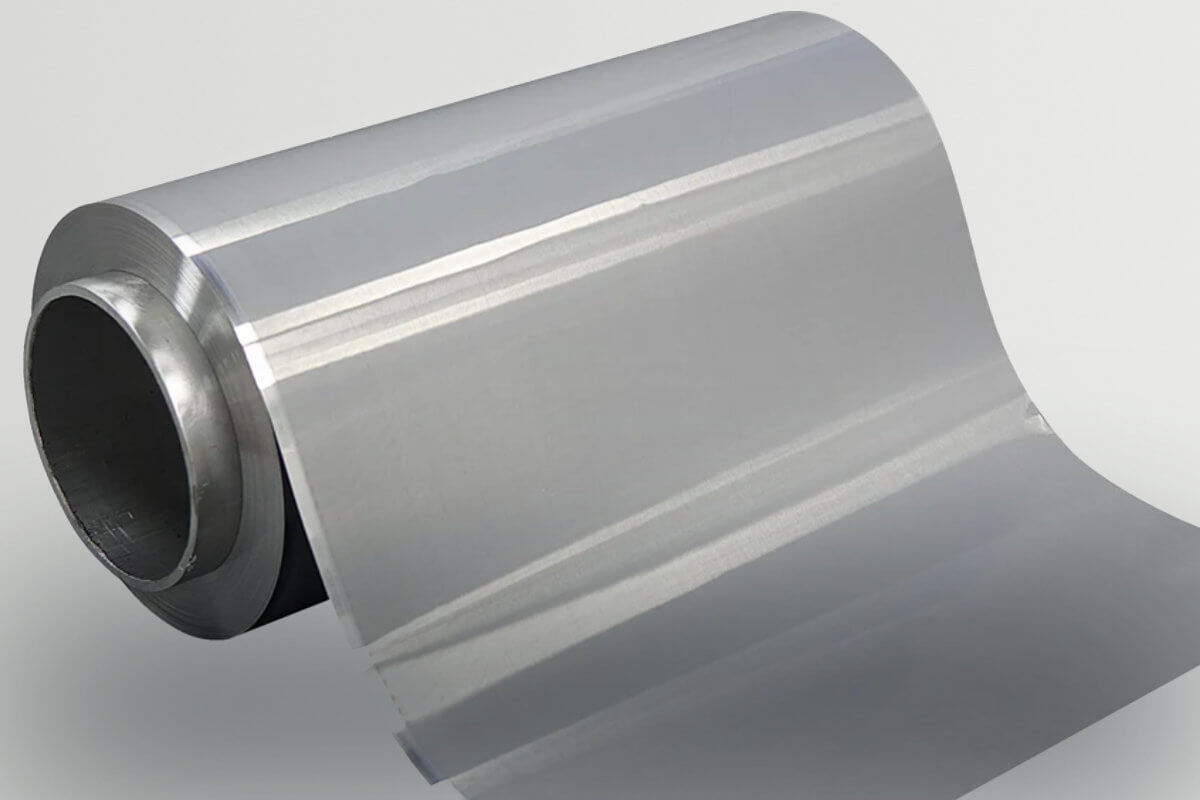
- Metal layers and wafer metallization
- De-icing and heating
- Batteries and fuel cells
- Coated paper and conductive textiles
- Graphene layers
- Antibacterial coatings
Data Table for EddyCus® inline
System Features
| Measurement technology | Non-contact eddy current sensor |
| Substrates | Boules, ingots, wafer, foils, glass, etc. |
| Measurement gap size | 3 / 5 / 10 / 15 / 25 / 50 mm (other upon request) |
| Number of sensor pairs / monitoring lanes | 1 – 99 |
| Sensor sizes (W x L x H) in mm | Sensor M: 80 x 100 x 66 Sensor S: 34 x 48 x 117 |
| Conductive layers | Metals/ TCOs/ CNTs/ nanowires/ graphene/ grids/ PEDOT/ others |
| Environment |
Ex-vacuo / in-vacuo @ T < 60°C / 140°F (higher on request) (for integrated temperature drift compensation for long term measurements) ATEX on request |
| Sample rate | 1 / 10 / 50 / 100 / 1,000 measurements per second |
| Hardware trigger | 24 V (5 or 12 V upon request) |
| Interfaces | UDP, TCP, .Net libraries, Modbus, Profinet, analog/digital, CSV, XML, other |
Measurement Capabilities
| Sheet Resistance Measurement | |
|---|---|
| This non-contact sheet resistance monitoring system measures in high speed and non-contact the sheet resistance directly in manufacturing processes. Typical processes involve PVD, CVD, galvanic or conventional deposition processes on wafer, foils, paper, polymers or other substrates. In particular these processes include sputtering, evaporation, epitaxy or plating processes. Additionally, this also involves spraying, slot die coating or electronic printing processes. Furthermore, sheet resistance enhancing processes such as annealing and doping of thin-films or sintering of printed electronics benefit from inline monitoring of the electrical integrity. Oxidation, etching, polishing and also the impact of cleaning and drying processes are also part of the wide application range of this state of the art testing technique. The sheet resistance values are typically transferred to MES systems for quality assurance and particularly for process control. | |
| Very low range sensor measurement range |
0.05 – 0.1 mOhm/sq @ < 3 % accuracy and repeatability < 0.5 % 0.1 – 10 mOhm/sq @ < 2 % accuracy and repeatability < 0.5 % 10 – 100 mOhm/sq @ < 3 % accuracy and repeatability < 1 % 100 – 300 mOhm/sq @ < 5 % accuracy and repeatability < 2 % |
| Low range sensor measurement range |
0.001 – 0.01 Ohm/sq @ < 2 % accuracy and repeatability < 0.3 % 0.01 – 1 Ohm/sq @ < 2 % accuracy and repeatability < 0.3 % 1 – 10 Ohm/sq @ < 2 % accuracy and repeatability < 0.5 % 10 – 100 Ohm/sq @ < 3% accuracy and repeatability < 1 % |
| Wide range sensor measurement range |
0.001 – 0.01 Ohm/sq @ < 2 % accuracy and repeatability < 0.3 % 0.01 – 0.1 Ohm/sq @ < 2 % accuracy and repeatability < 0.3 % 0.1 – 10 Ohm/sq @ < 2 % accuracy and repeatability < 0.3 % 10 – 100 Ohm/sq @ < 2 % accuracy and repeatability < 0.5 % 100 – 500 Ohm/sq @ < 3 % accuracy and repeatability < 1 % 500 – 1,000 Ohm/sq@ < 3 % accuracy and repeatability < 1 % |
| High range sensor measurement range |
100 – 500 Ohm/sq @ < 5 % accuracy and repeatability < 3 % 500 – 1,000 Ohm/sq@ < 3 % accuracy and repeatability < 2 % 1,000 – 10,000 Ohm/sq @ < 3 % accuracy and repeatability < 1 % 10,000 – 50,000 Ohm/sq @ < 3 % accuracy and repeatability < 1 % 50,000 – 200,000 Ohm/sq @ < 3 % accuracy and repeatability < 1 % |
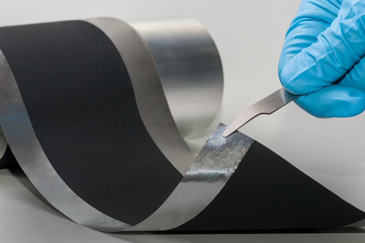
Metal Layer Thickness Measurement |
| This non-contact metal thickness monitoring system provides immediate feedback for layer deposition and layer removal manufacturing processes. Typical deposition processes include sputtering, evaporation, plating or atomic layer deposition (ALD) e.g. on wafer, foils, glass, ceramics (e.g. PCT), paper, polymers or other substrates. Layer removal processes include polishing (CMP) or etching or laser scribing. The technical concept includes reflective and transmission eddy current sensors and sensor setups. Additionally, a wide range of interface options are supported. | |
| Sheet resistance range | Direct thickness calibration / sheet resistance conversion |
|
Metal thickness range Accuracies depend on the selected setup and the type / conductivity of the metal (e.g. copper, aluminum, silver) |
Low 1 – 10 nm; 2 – 5 % accuracy Standard 10 – 1,000 nm; 1 – 3 % accuracy High 1 – 100 µm; 0.5 – 3 % accuracy |
Electrical Anisotropy Measurement |
| The ability for non-destructive and non-contact inline measurement of electrical anisotropy is a unique capability of SURAGUS. The inline A series induces currents in two or four directions and measures simultaneously the sheet resistance in different directions. The two-direction mode is used for most inline applications. Here the machine direction is the known to be the dominant alignment direction for process reasons and flow of deposition material. If the dominant alignment direction of conductive material is not known, then the four-sensor setup is applied. This sensor series is used for slot die or spray coating, screen printing or spinning processes. Typical materials are Silver nanowires, nanotubes or nanobuds, anisotropic meshes or structures or materials with anisotropic domain sizes or layer (stacks) with advanced current transport functions. The monitors are used to control isotropy or to achieve dedicated anisotropies where current transport is to be optimized in certain directions. In some case those systems are used to measure on structured materials or to identify defects. | |
| Sheet resistance range | 0.01 – 1,000 Ohm/sq; 1 – 5 % accuracy |
| Anisotropy range (TD/MD) | 0.33 – 3 (larger upon request) |
| Materials |
Nanowires Nanotubes / Nanobuds Regular metal meshes Materials with egg shaped domains Stacked multilayer systems with advance current transport functions |
| Measurement Results |
Absolute / relative anisotropy Dominant current transport directions Sheet resistance in machine direction Sheet resistance in traversing directions (cross-web) |
Wet Coating and Residual Moisture Measurement |
| The HF series utilizes high frequency (HF) electromagnetic fields that interact with layers utilizing different effects. Those systems are used to analyze dielectrical and electric properties. Applications include the measurements such as residual moisture and layer thicknesses of wet coatings. Processes include spray, slot die coating, curtain coating and many more wet deposition processes. Additionally drying and calendaring processes can be controlled. | |
| Testing parameters |
Residual Moisture Material composition (conductive vs dielectric vs magnetic elements) Wet coating thickness |
Substrates | Foils, glass, pipes, various containers and transport items |
| Measurement types |
Wet thickness (µm) Weight (g/m²) Drying status (%) Conductivity (MS/m) Resistivity (mOhm·cm) Permeability (H/m) Beta Permittivity (F/m) Beta |
| Measurement range / accuracy |
Depends on the measurement task and the material composition and test object volume. Please consult with the SURAGUS team |
| Environment |
Ex-vacuo In-vacuo ATEX on request T < 60°C (higher upon request) |
Resistivity and Conductivity Measurement |
| The EddyCus® inline RM sensors measure the resistivity or conductivity or related parameters in automated handling or processing tools and manufacturing lines. Materials include semiconductors such as Si, SiC, GaAs, GaN, SiSiC and metals and alloys or other conductive materials. Applications in PV or semiconductor industry include wafer, boule or ingot characterization. Even further, temperature measurement of wafer, metals and metal sheets can be obtained by exploiting the correlation of temperature to resistivity. Bulk or volume materials are characterized with reflective mode sensors. Various penetration depth levels can be achieved by sensor and frequency variation. Further applications include integrity imaging of structured films or printed electronics on 3D shapes. | |
| Penetration depth | 10 µm to 10 mm (depending on conductivity and measurement frequency 10 kHz to 50 MHz cf. technology page) |
| Spot size | Various sensors are available. Coil size is 875 µm to 100 mm |
| Substrates | Wafer, metals, alloys, ceramics, plastics etc. |
| Materials | Semiconductors, metals, alloys, conductive polymers, conductive ceramics |
| Measurement mode | Single side reflection mode or transmittance mode with total thickness measurement |
| Conductive layers | Metals/ TCOs/ CNTs/ nanowires/ graphene/ grids/ PEDOT/ others |
| Resistivity range | 0.1 – 1,000 mOhm·cm |
| Conductivity range | 0.01 – 65 MS/m |
|
Metal thickness range Accuracies depend on the selected setup and the type / conductivity of the metal (e.g. copper, aluminum, silver) |
Low 1 – 10 nm; 2 – 5 % accuracy Standard 10 – 1,000 nm; 1 – 3 % accuracy High 1 – 100 µm; 0.5 – 3 % accuracy |
Frequently Asked Questions
Sheet resistance, metal layer thickness, resistivity, electrical anisotropy, wet coating and residual moisture
- EddyCus® inline SR – Sheet resistance monitoring (incl. emissivity)
- EddyCus® inline MT – Metal thickness monitoring
- EddyCus® inline RM – Resistivity and conductivity monitoring
- EddyCus® inline HF – Residual moisture monitoring
- EddyCus® inline A – Sheet resistance and electrical anisotropy monitoring