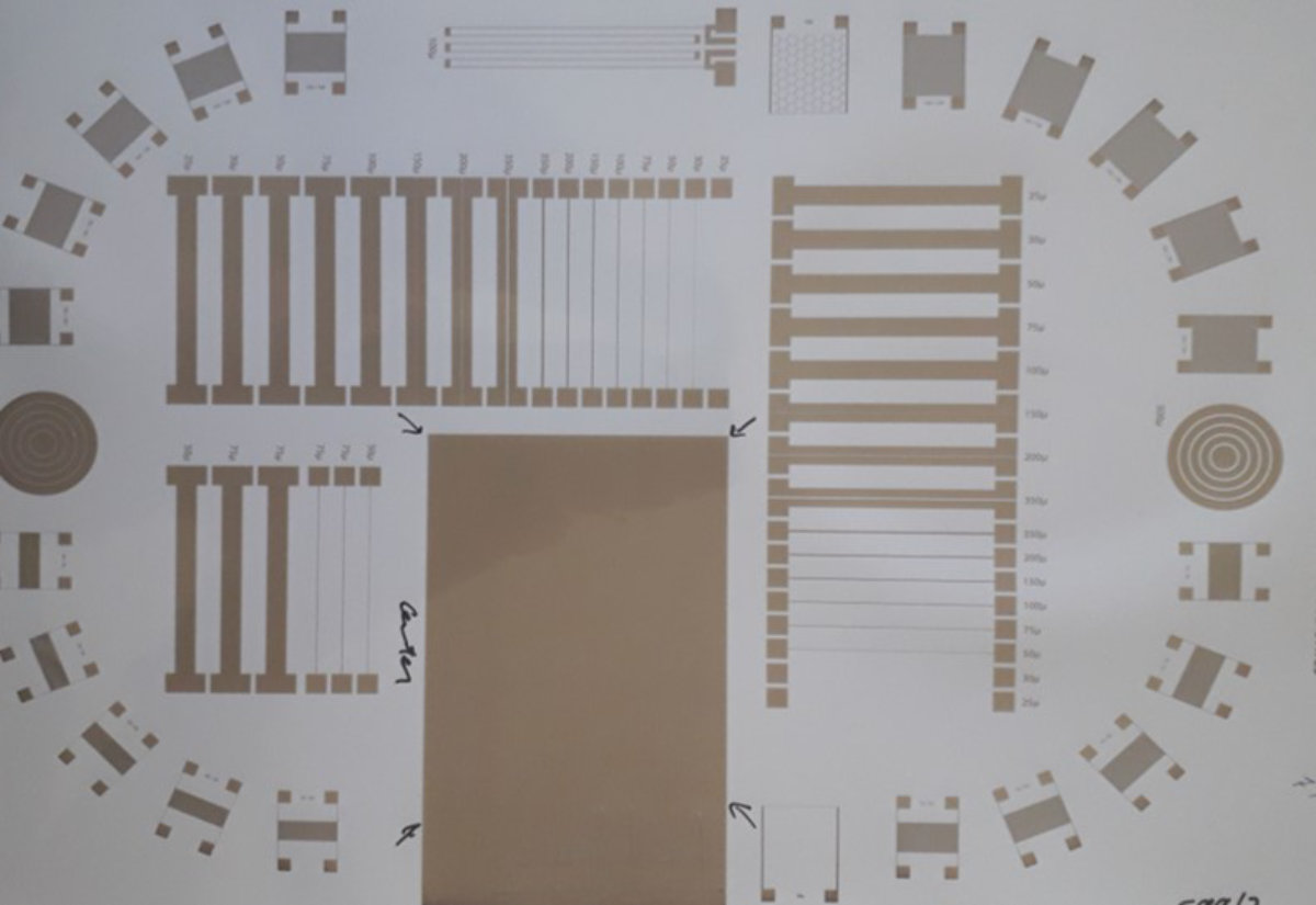
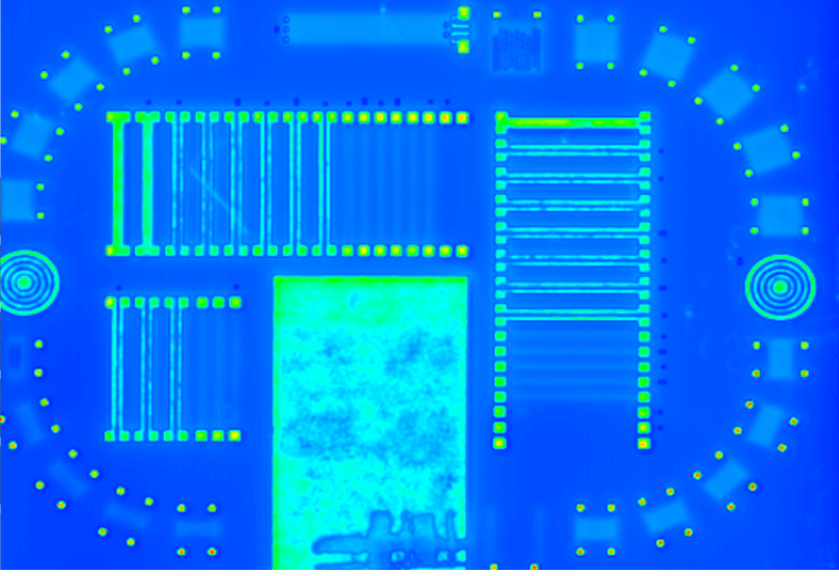
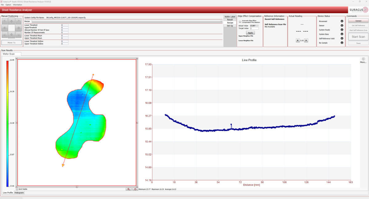
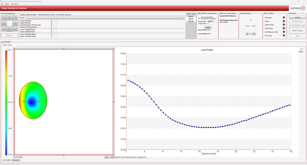
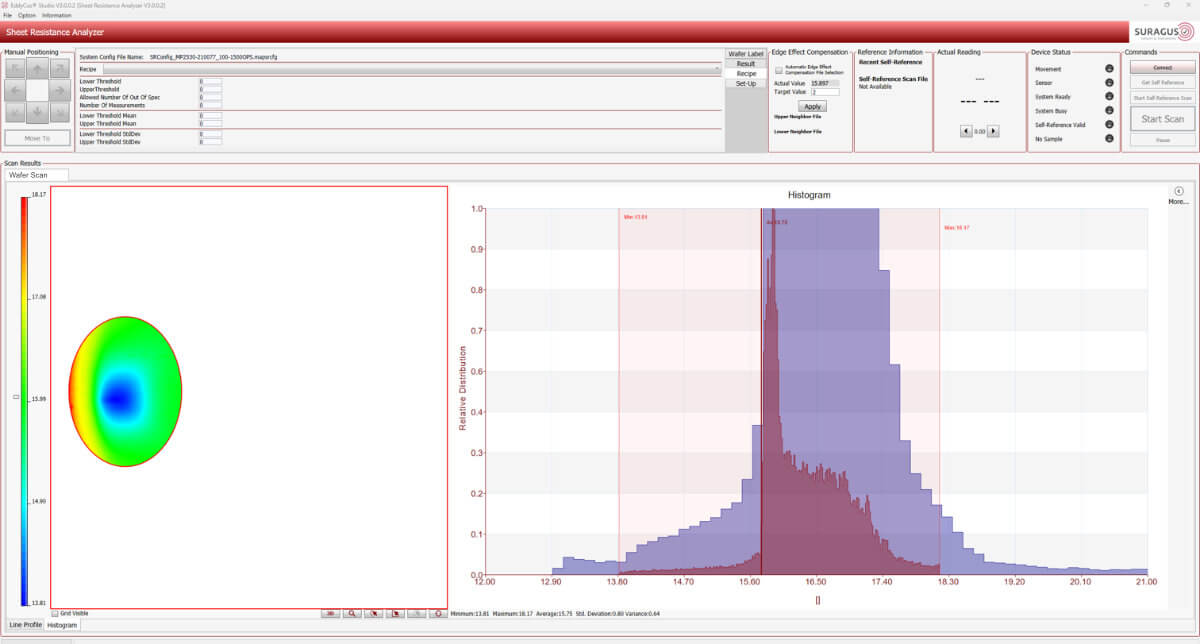
Multi Application Imaging Device
Higher Thin-film and substrate quality through fast and precise mapping devices based on non-contact eddy current technology.
- High resolution images with over 30 000 measurement points within 4 minutes for best defect detection
- Measurement up to the edge of the sample
- Various analyzing options such as line profiles or histogram
- Various sensor options to adjust the device optimal to your measurement task
Introduction
The EddyCus® map 2530 RMT for mixed solutions is a bench top scanner particularly suitable for research and technology labs. It is fully functional to measure a bunch of different applications such as solar wafers, printed electronics and carbon fibers. It’s a compact device, which can measure samples up to 300 mm (12 inch).
The device is typically used for:
- Printed electronics
- Solar wafer
- Carbon fiber

Sensor Capabilities
- Resistivity [0.1 – 1,000 mOhm·cm]
- Conductivity [0.01 – 65 MS/m]
- Sheet Resistance [0.05 mOhm/sq – 100 Ohm/sq]
- Metal Layer Thickness [by conversion or direct calibration]
- Distance [1 – 3,000 µm]
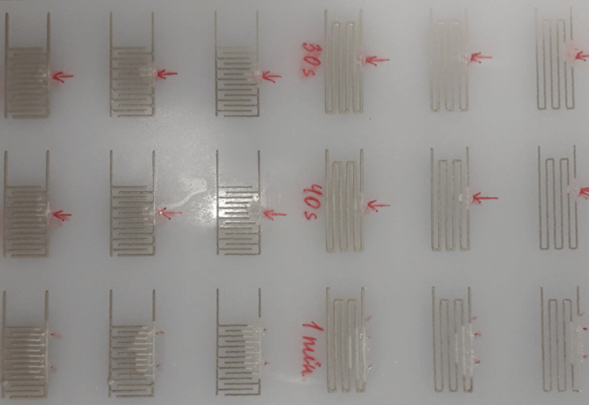
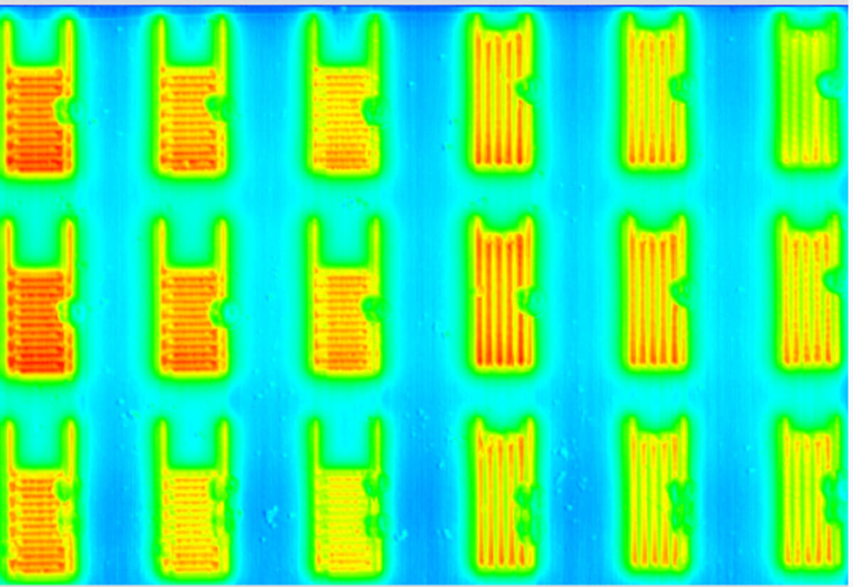
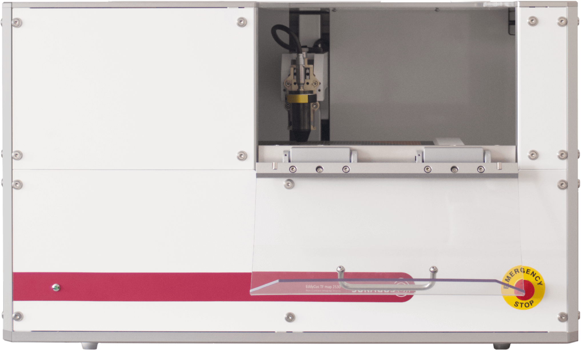
Supported Substrates
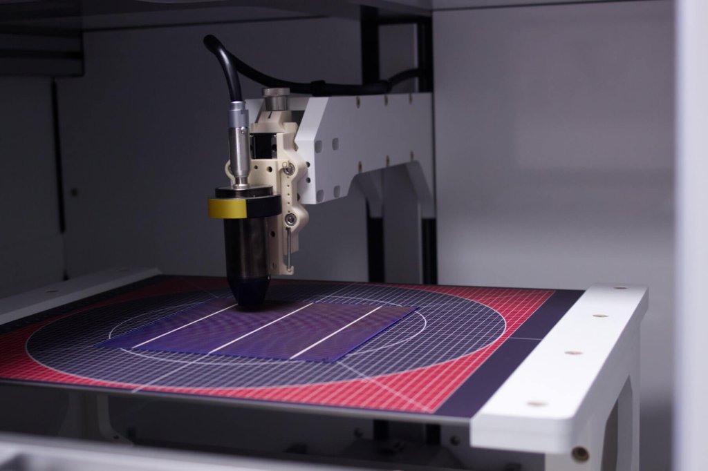
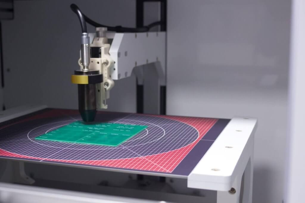
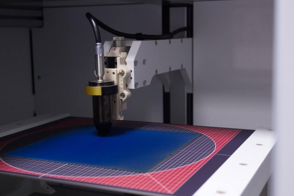
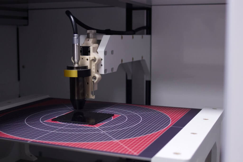
Flat or slightly curved objects suuch as solar wafer,
printed electronics, carbon fibers
- Maximum height: 100 mm
- Maximum weight: 10 kg
Measurement Field
Sample sizes between Ø 150 mm and Ø 200 mm
Individual sizes upon request
Applications


Printed Electronics Application
A visual inspection of printed electronics is not sufficient to ensure their functionality. The EddyCus® map RMT for mixed solutions can assess the integrity of printed electronics and detect inconsistencies—even when, as shown in the two images below, no defects are visible to the naked eye after optical inspection.


Example Photo and Corresponding Scan of a Test Structure of Printed Electronics
This example showcases printed electronic test structures alongside high-resolution eddy current mapping performed by the EddyCus® map 2530 RMT for mixed applications.
Example Photo of Printed Device and Eddy Current Scan
This example shows printed devices with defects. The eddy current image was done by high-resolution eddy current mapping device EddyCus® map 2530 RMT for mixed applications.


Example Photo of Printed Fine Structure and Eddy Current Imaging
This examples shows a printed fine structure and its high resolution eddy current scan.
Solar Wafer Application
The EddyCus® map 2530 RMT for mixed applications imaging device can measure samples with heights of up to 40 mm and a maximum curvature of 10 mm. The device supports sample weights of up to 5 kg (depending on the diameter). If you need to measure heavier samples, please contact us for more information.
- Solar wafer
- Thin film pv
- Crystalline solar cell


Sample Scan of a Crystalline Solar Cell
The scan shows the conductive structures of the solar cell.
Easy to Use Software With Various Analyzing Options
The EddyCus® map 2530 RMT for mixed solutions has an easy to use software. After you laid your sample central on the measurement field you
- Choose your recipe
- Press on “Start”
- Watch the software creating the map while scan process proceeds
After the scan is finished you can start the analyzing process. You will be able to
- Draw line profiles
- Predefined line profiles and
- Free drawed line profiles
- Draw specific areas of interest
- Rectangle
- Circle
- Pen to draw free area
- Select a histogram
Sheet Resistance Imaging
Metal Layer Thickness Imaging
Resistivity Imaging
Electrical Anisotropy Imaging
Video of the EddyCus® map 2530 RMT
The video gives you an impression of how to use the Portable. Which materials can be analysed and how the device works in general.
Data Table for EddyCus® map 2530 RMT – Mixed Solutions
Device Features
Measurement technology | High frequency eddy current sensor |
Substrates | Solar wafer, carbon, pcb, printed electronics |
Max. scanning area | 12 inch / 300 mm x 300 mm |
Edge effect correction / exclusion | 2 – 10 mm (depending on size, range, setup and requirements) |
Max. sample thickness / sensor gap | 40 mm |
Pitch | 0.1 – 10 mm |
Spot size (coil size) Penetration depth (frequency) |
0.1 / 1 / 2.5 / 5 / 10 mm (other upon request) |
Spot size (coil size) Penetration depth (frequency) |
1 – 9 mm (depending on coil size) 1 – 10 mm (depending on frequency) |
Measurement points per time (square shaped samples) | 100 measurement points in 0.5 minutes 10,000 measurement points in 3 minutes |
Speed | 150 mm per second (time 1 to 30 minutes) |
Available measurement features | Sheet resistance map Conductivity map Resistivity map Electrical anisotropy map Permeability map (beta) |
Device dimensions (w/h/d) | 31.5” x 19.1” x 33.5” / 785 mm x 486 mm x 850 mm |
Weight | 90 kg |
Measurement Capabilities
Sheet Resistance Measurement | |
---|---|
Sheet resistance range | 0.0005 – 100 Ohm/sq |
Accuracy | 1 – 3 % |
Repeatability | 0.5 – 1.5 % | Resistivity Measurement |
Resistivity range | 0.1 – 1,000 mOhm·cm |
Accuracy | 1 – 3 % |
Repeatability | 0.5 – 1.5 % | Conductivity Measurement |
Conductivity range | 0.01 – 65 MS/m |
Accuracy | 1 – 3 % |
Repeatability | 0.5 – 1.5 % | Non-conductive Coating Measurement |
Distance range | 1 – 3,000 µm |
Accuracy | Shown in feasibility study |
Repeatability | Shown in feasibility study |
Frequently Asked Questions
Sheet resistance, metal layer thickness, resistivity, conductivity
50 mm – 300 mm samples (others on request)