Sensor Capabilities
- Sheet Resistance [0.01 – 1,000 Ohm/sq]
- Metal Layer Thickness [5 nm – 2 mm]
- Resistivity [0.1 – 100 mOhm·cm]
- Wafer Temperature
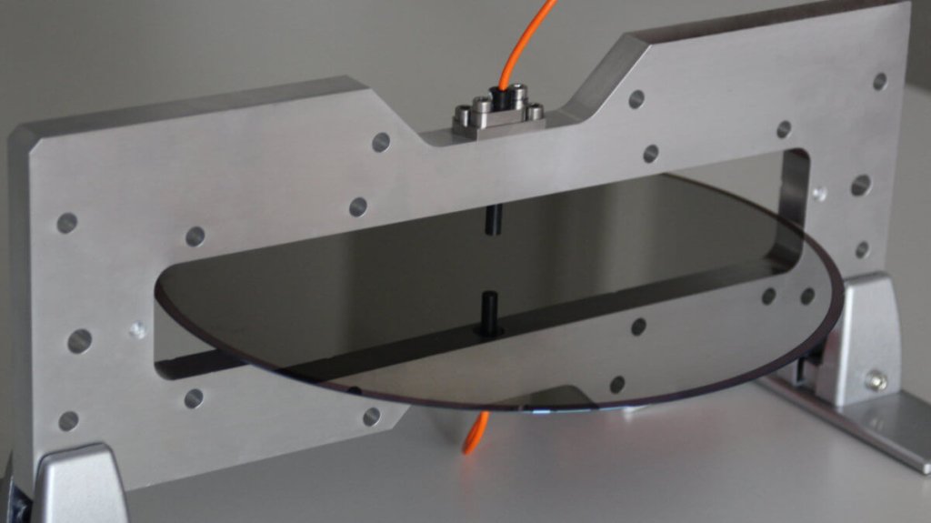
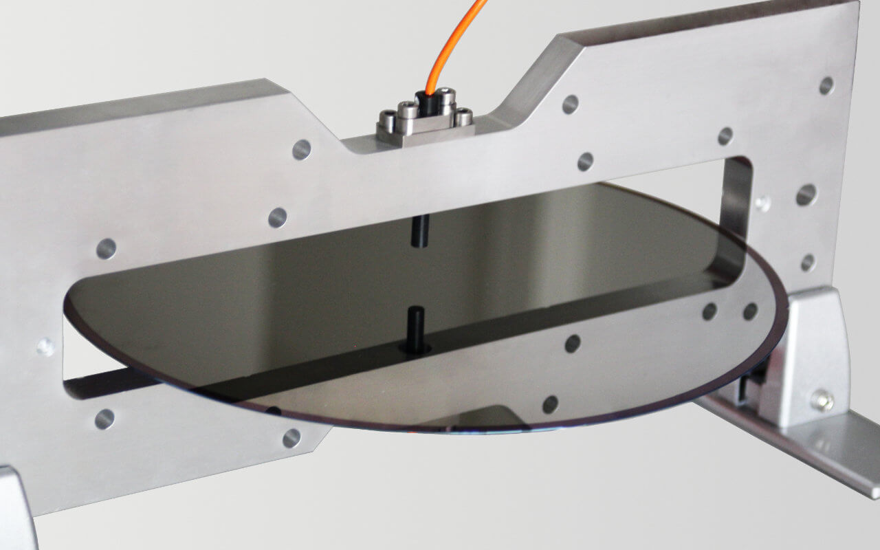
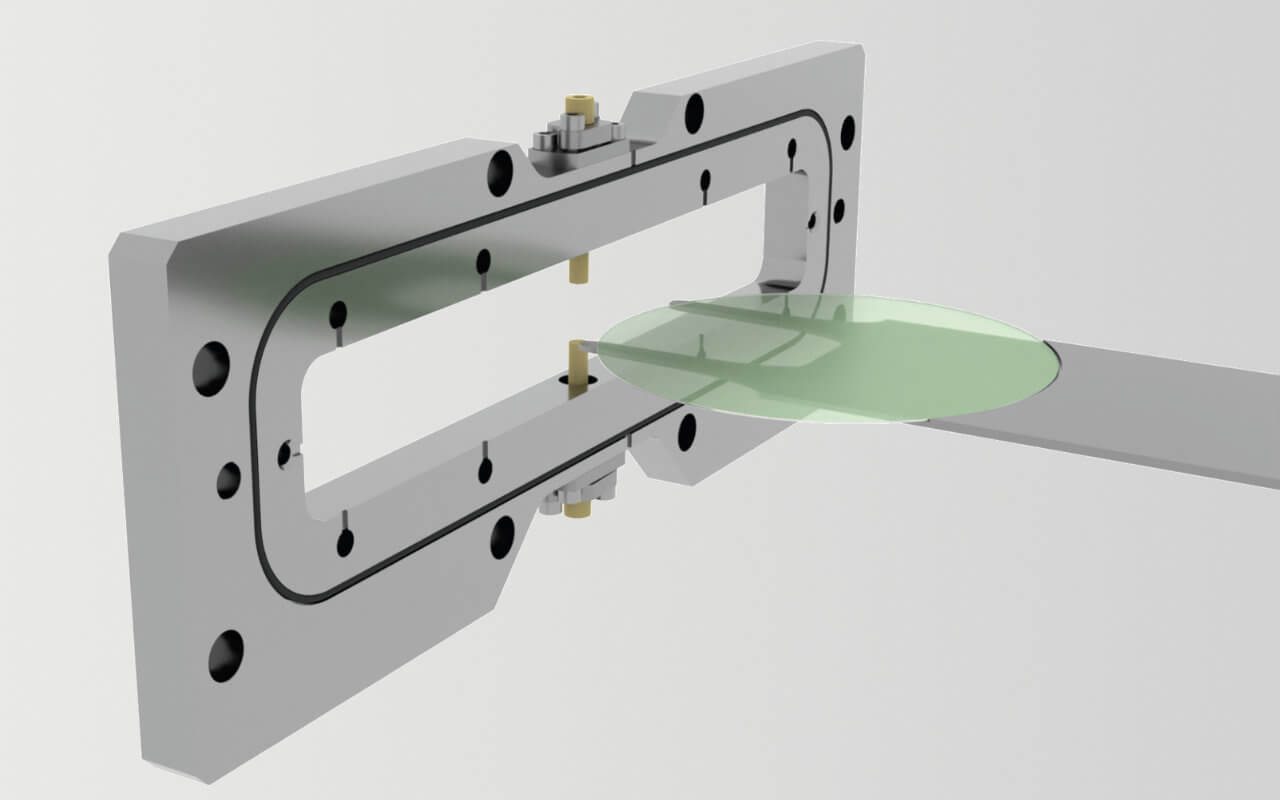
Gap Size
5 – 50 mm (depending on wafer handler)
Supported Substrates
150 – 300 mm Wafer
Supported Interfaces
- UDP
- PROFINET
- TDP
- .Net libraries
- Modbus (upcoming)
- EtherCAT (upcoming)
Supported Sizes
- 150 mm
- 200 mm
- 300 mm