Mapping of Wafers
and Metallization Layers
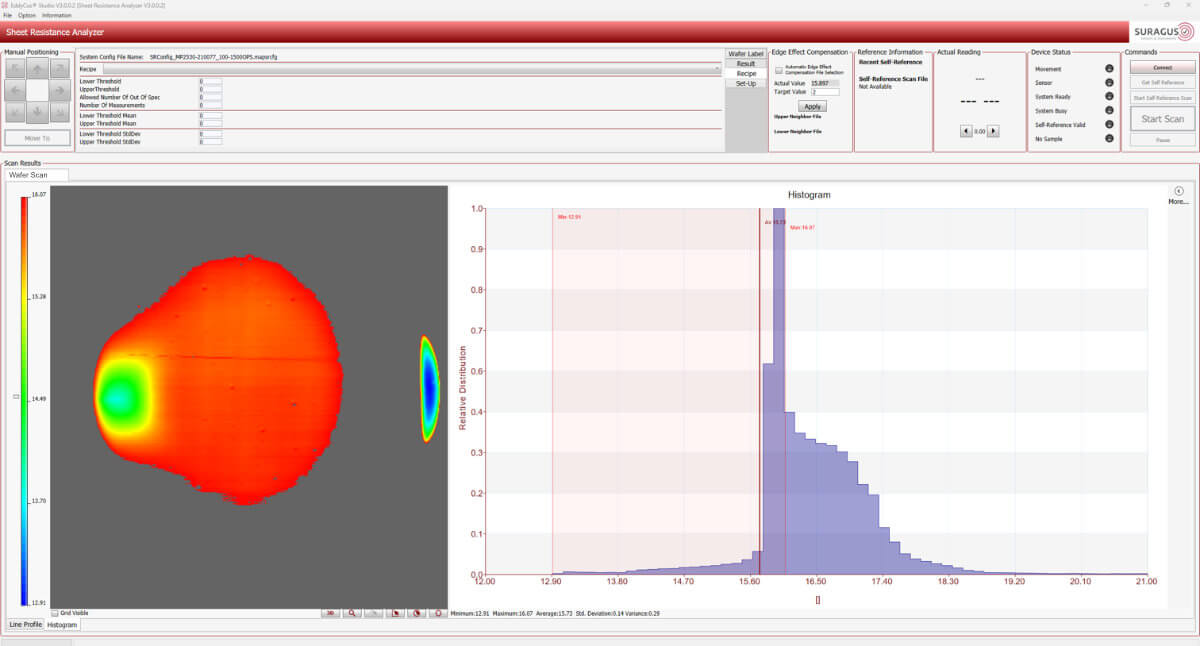
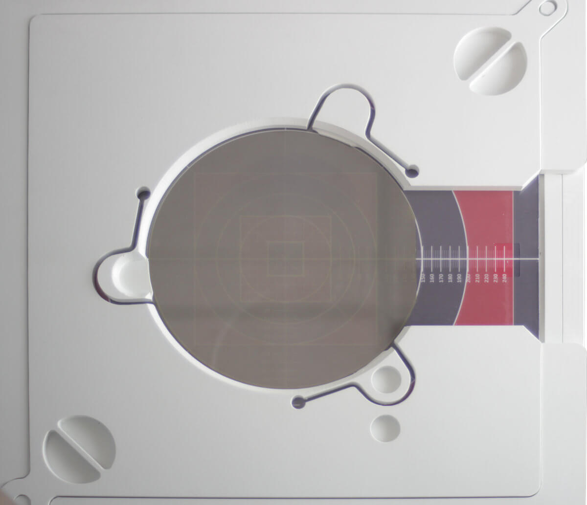
Improved thin-film and substrate quality is achieved through high-resolution mapping enabled by non-contact eddy current technology. The EddyCus® map 2530 RMB, with its minimal spot size, allows for precise measurements in close proximity to the sample edge.
- Non-contact
- Fast and precise measurement
- High resolution mapping of conductive thin films
- Imaging of substrates up to 220 x 220 mm (8 x 8 inches)
- Characterization even of hidden and encapsulated conductive layers
- Various software-integrated analysis functions (e.g. sheet resistance distribution, line scans, single point analysis)
- Measurement data saving and export functions
- Defect detection and coating analysis
Introduction
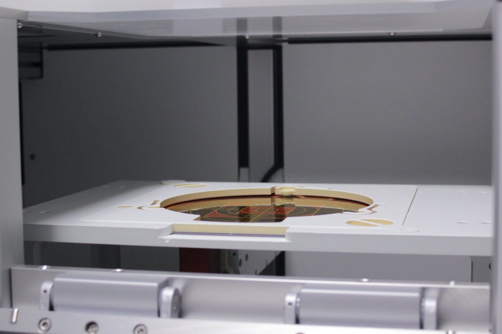
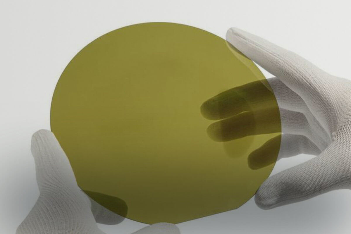
The EddyCus® map 2530 RMB is a non-contact eddy current mapping system specifically optimized for the high-resolution electrical characterization of semiconductor wafers and their metallization layers. Tailored for applications requiring minimal penetration depth, this system is equipped with compact sensors that enable exceptionally small spot sizes—ideal for detailed mapping of thin conductive layers and localized features, including near-edge regions of wafers.
Although optimized for wafers, the system can also accommodate small bulk samples such as boules or pucks with dimensions up to 50 mm in height and 100 g in weight, providing added flexibility for R&D and quality control workflows.
Designed to deliver spatially resolved imaging of key electrical parameters—such as sheet resistance, bulk resistivity, and derived conductivity metrics—the EddyCus® map 2530 RMB enables precise visualization of material homogeneity, dopant distribution, metallization uniformity, and defect structures. It supports advanced eddy current imaging (C-Scan) with a selectable measurement pitch ranging from 100 µm to 10 mm, and is capable of scanning 2D and 2.5D sample areas up to 220 × 220 mm (8 × 8 inches).
The system can be pre-configured from a range of sensor heads to suit different application requirements: high-resolution mapping for thin films and metallization layers, high-penetration probes for bulk analysis.
The device is typically used for:
- Wafer resistivity imaging
- Wafer metallization thickness or sheet resistance imaging
- Specimen sizes : 50 x 50 mm to 300 x 300 mm
- Various sensors dedicated to specific measurement task
- Customized specimen holder in terms of layout and shape in favor to specimen dimensions
- Data analysis, export and reporting functions
Sensor Capabilities
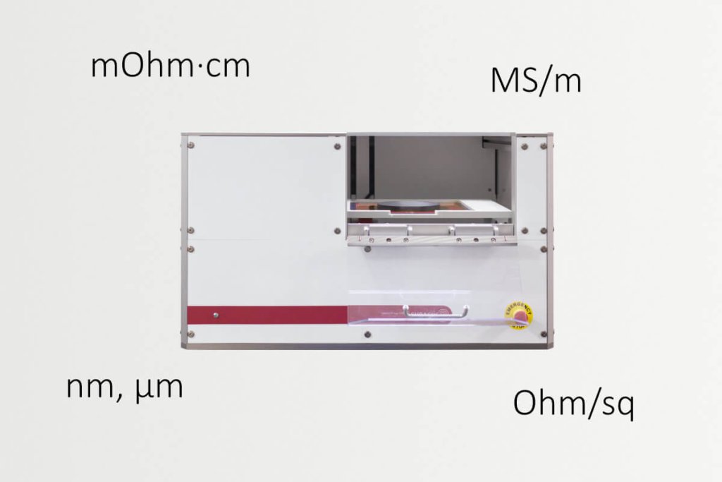
- Resistivity [0.1 – 100 mOhm·cm]
- Sheet Resistance [0.00005 – 10 Ohm/sq]
- Metal Layer Thickness [by conversion or direct calibration]
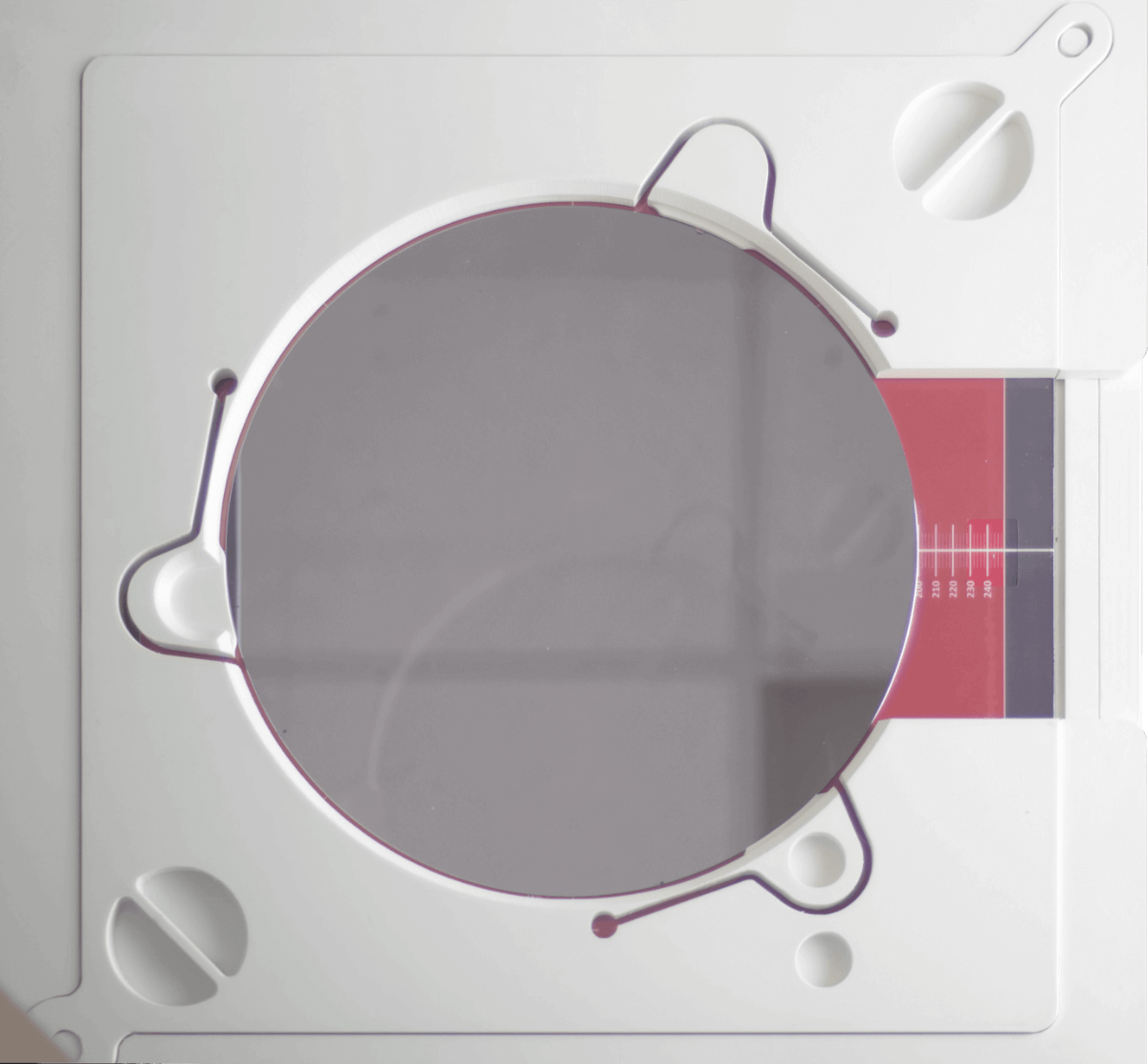
Wafer Retainer Inlays
- Sample sizes between ⌀ 50 – 300 mm
- Max. measurement area 220 mm x 220 mm
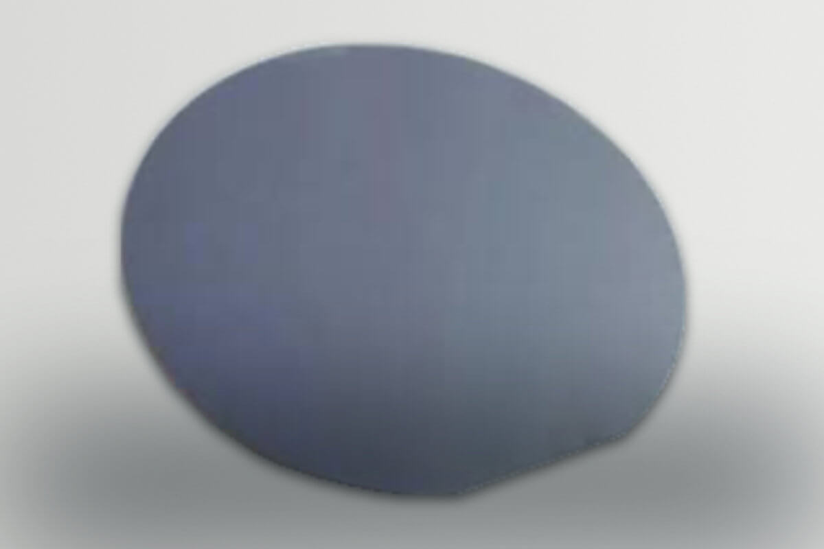
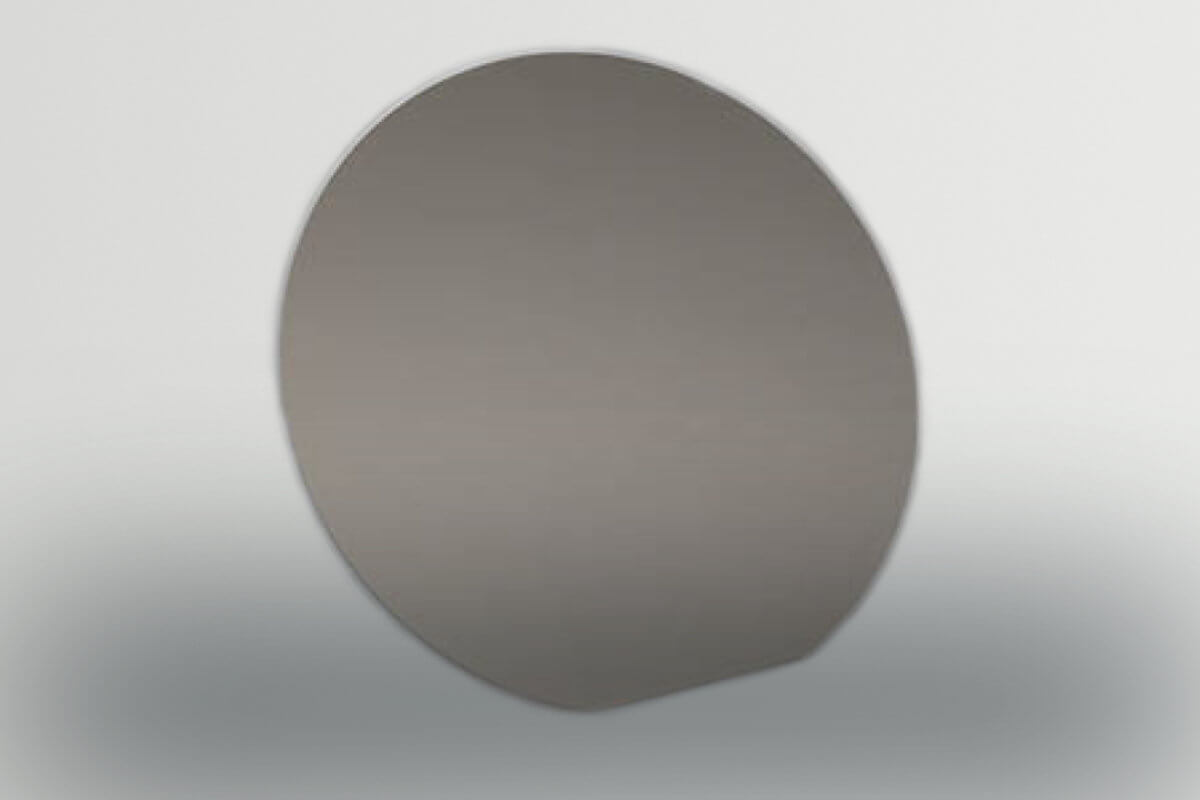
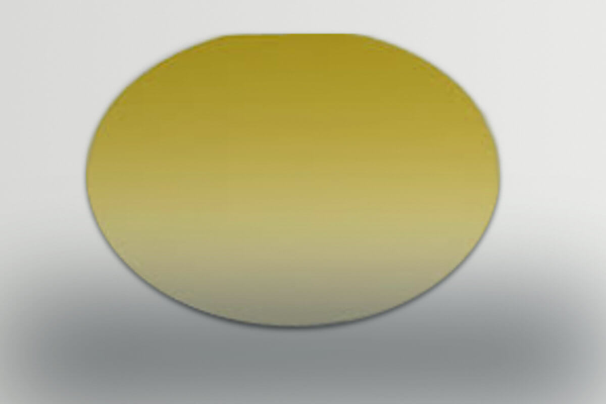
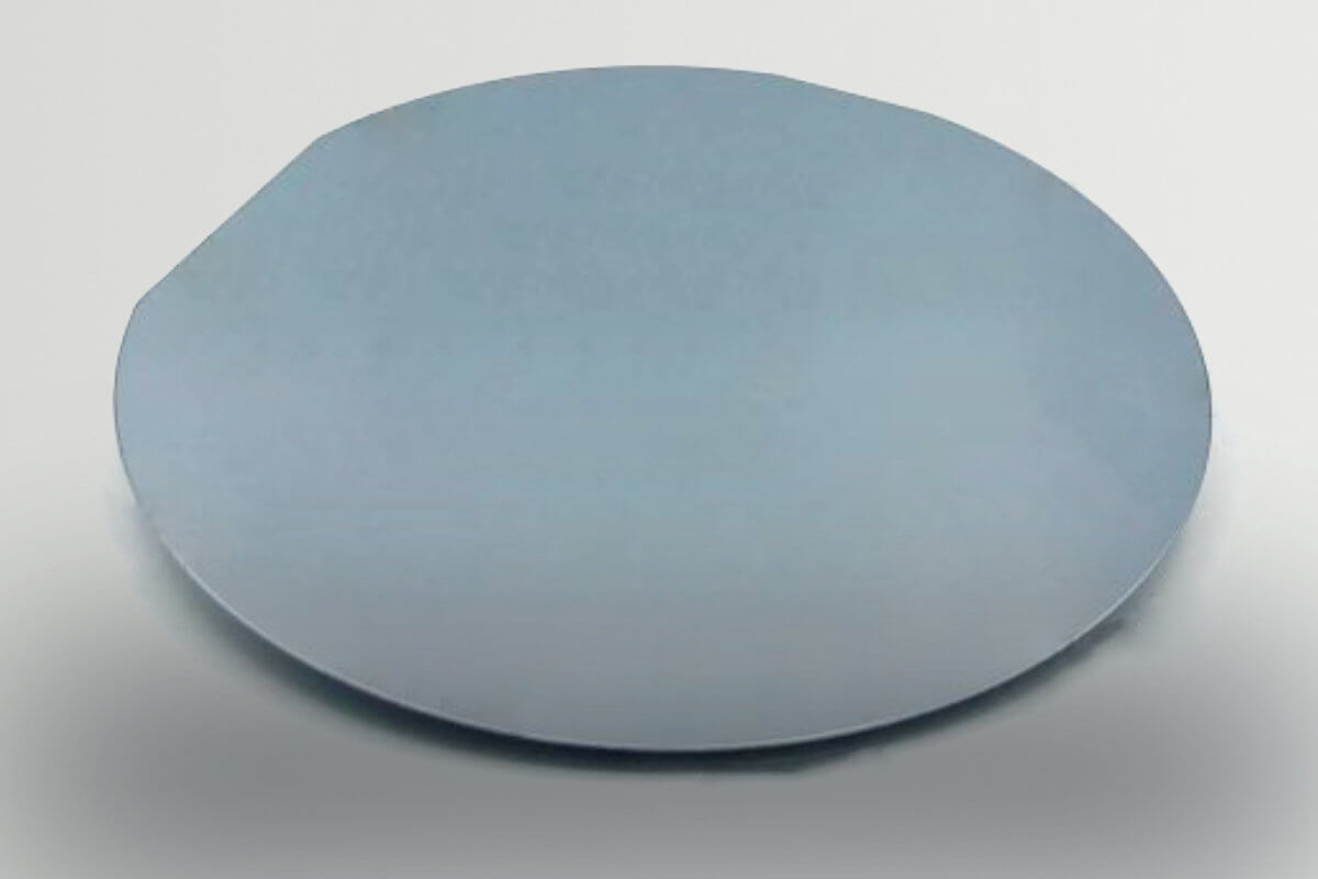
Supported Substrates
- Wafers
- Pucks and Boules up to 50 mm and 0.3 kg
Features and Benefits
2 – 12 Inch Wafers, Pucks and Boules
5 – 50 mm Puck or Boule Thickness
Various Analyzing Options
Fast Results
High Resolution Mappings
Easy To Use
One Device, Multiple Measurement Parameters
The EddyCus® map 2530 RMB is able to measure different measurement parameters. The resistivity correlates with sheet resistance and metal layer thickness. As long as the material is well known all of these measurement parameters can be measured precisely.
- Sheet resistance
- Metal layer thickness
- Resistivity
- Conductivity
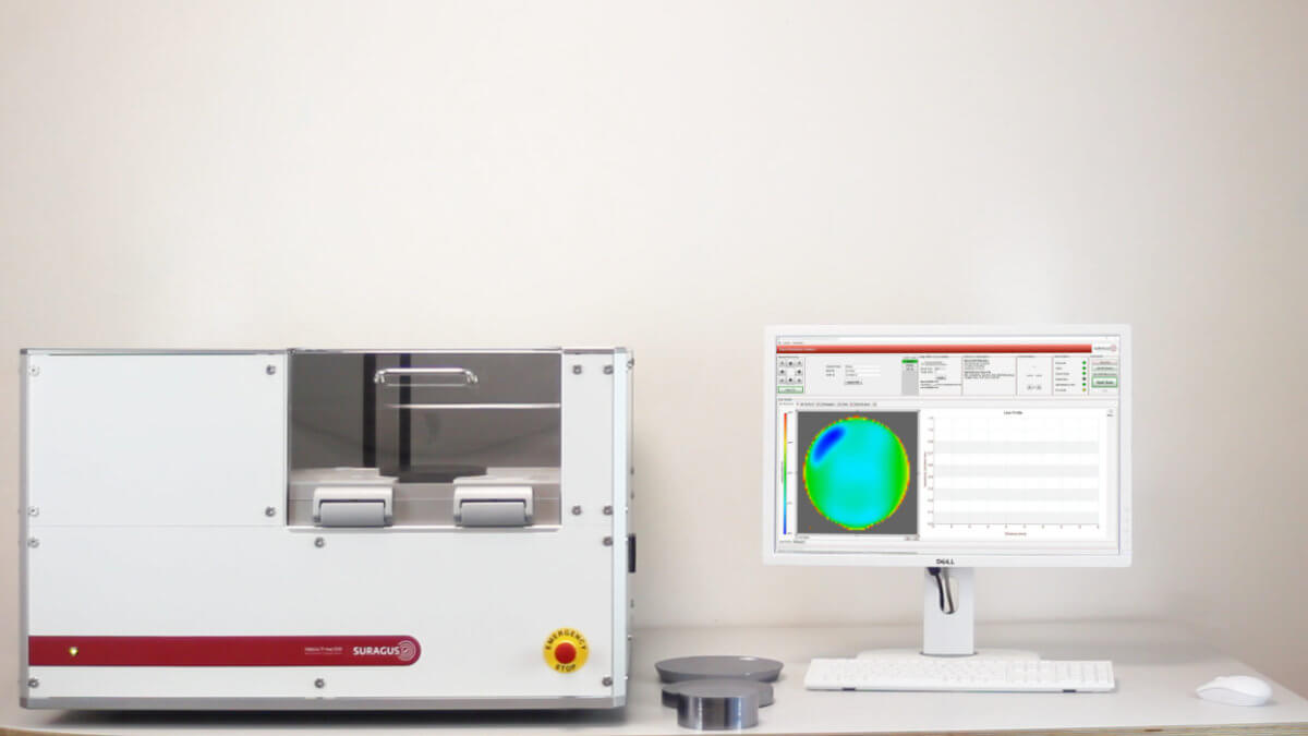
Software and Device Control
- Very user-friendly software
- Realtime mapping measurement
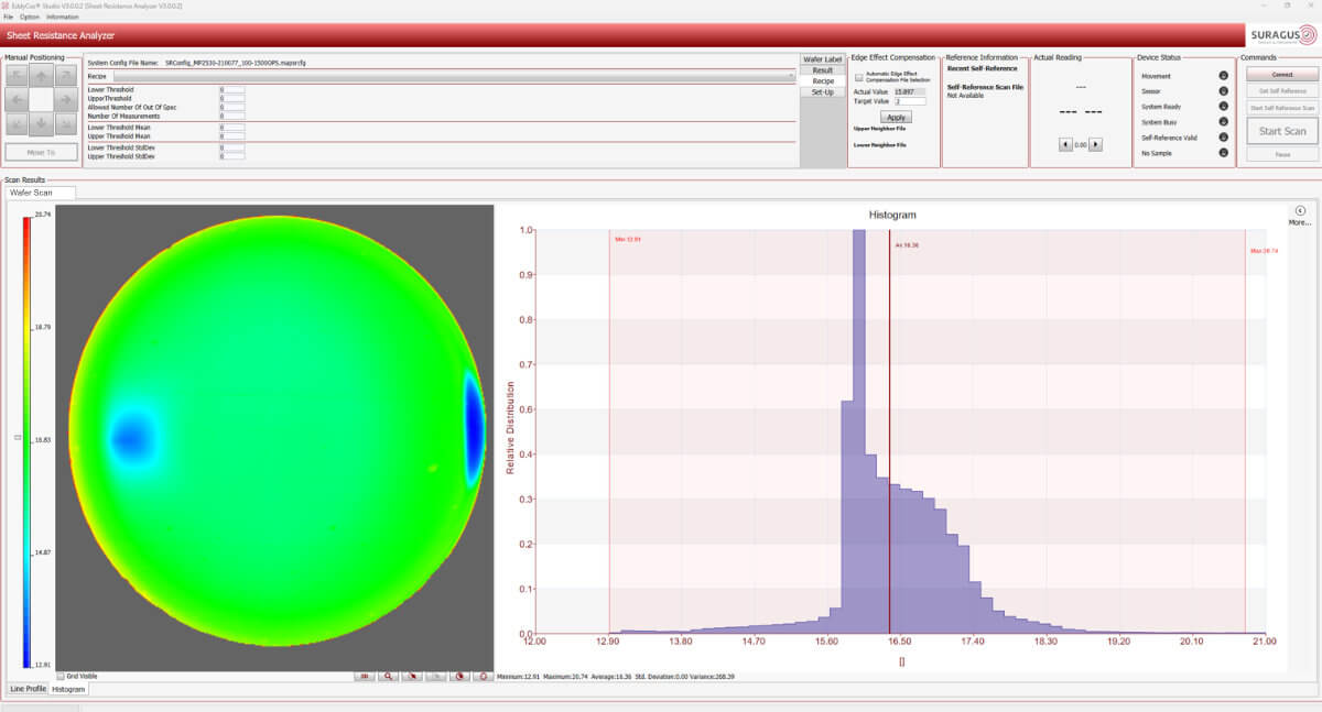
- Easy-to-use statistical analysis options
- Pre-defined measurement and product recipes (sizes, pitches, thresholds)
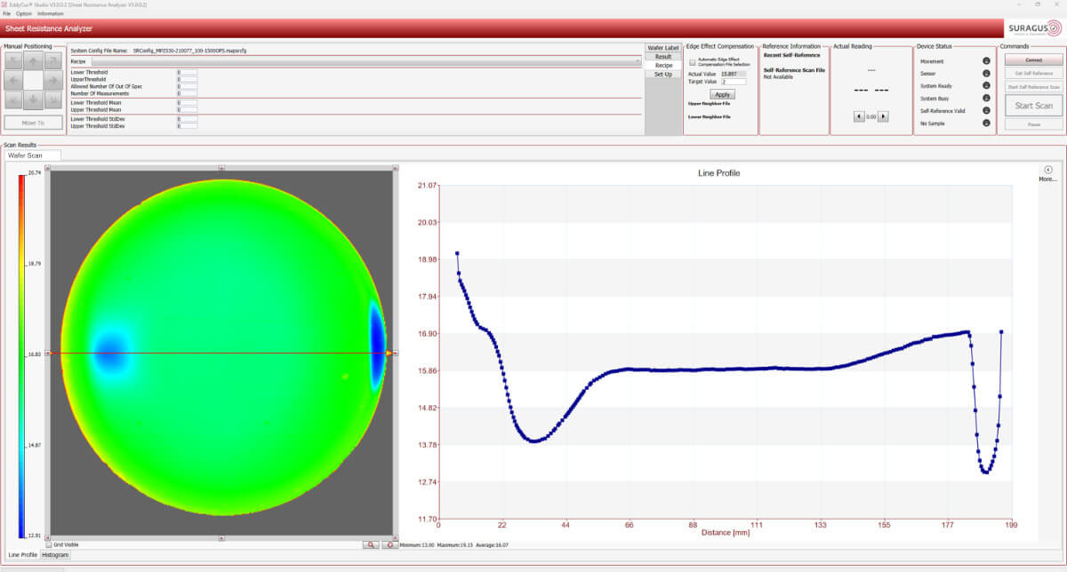
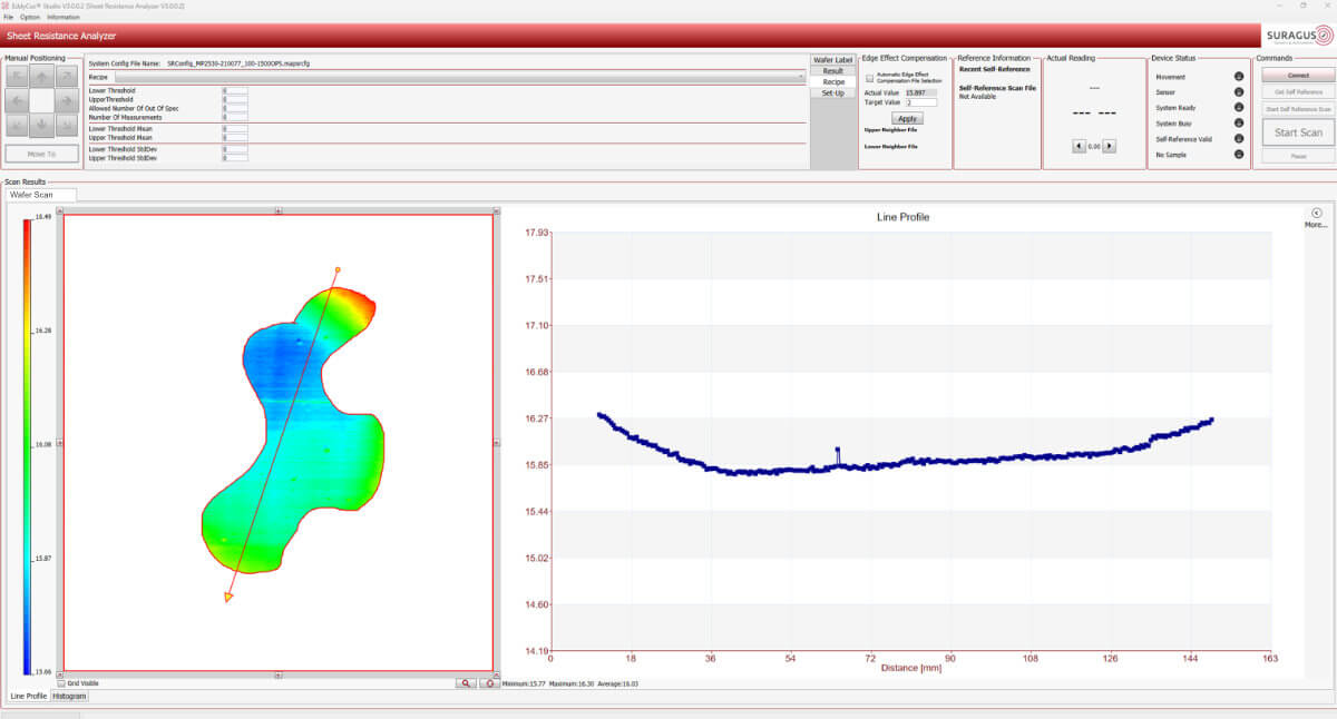
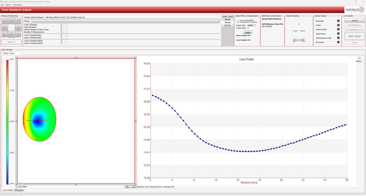
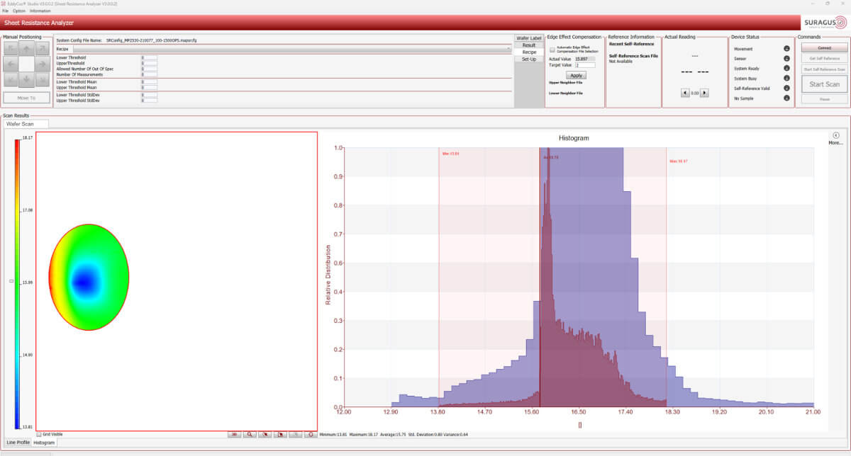
- Line scan, histogram and area analysis
- Black and colored image coding
- Csv & pdf export
- PC summary and export
- 3 user level
- Material database for parameter
- conversion
- Edge effect compensation
- Storage and import of data
- Export of data sets (e.g. to EddyEva, MS Excel, Origin)
Video of the EddyCus® map 2530 RMB
The video gives you an impression of how to use the map 2530 RMB. Which materials can be analysed and how the device works in general.
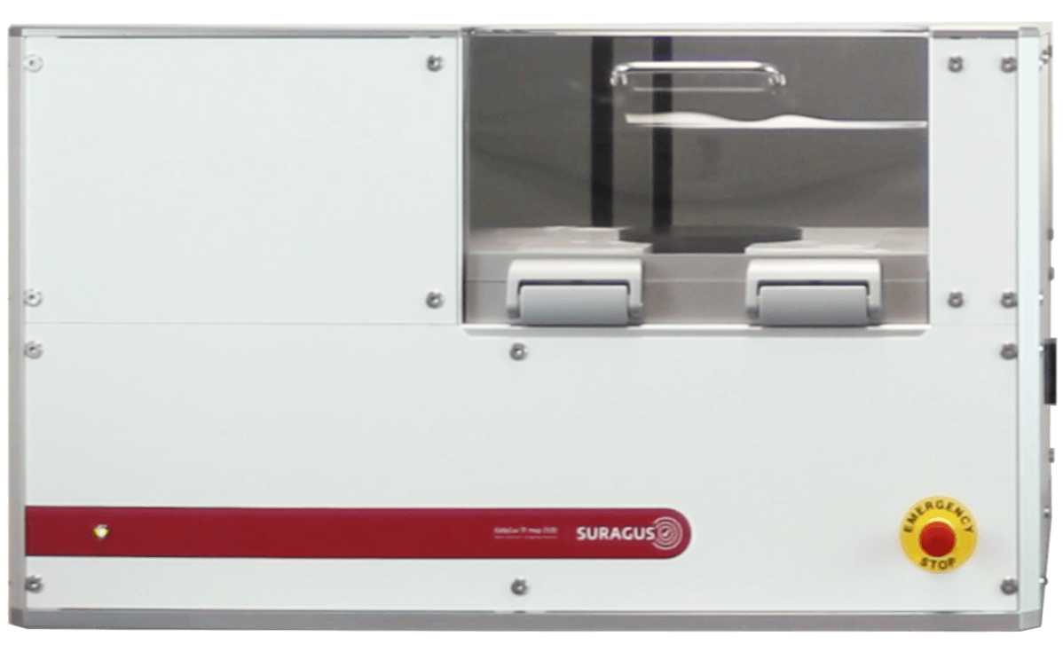
Data Table for EddyCus® map 2530 RMB
Device Features
| Measurement technology | High frequency eddy current sensor |
| Substrates | Wafers and bulk materials |
| Substrate area | 12 inch / 300 mm x 300 mm (larger upon request) |
| Movement area | 8 inch / 220 mm x 220 mm (larger upon request) |
| Edge effect correction / exclusion | 2 – 10 mm (depending on size, range, setup and requirements) |
| Max. sample thickness | 50 mm (max. 0.3 kg) |
| Scanning pitch | 0.1 / 1 / 2.5 / 5 / 10 / 25 mm (other upon request) |
| Speed | 400 mm per second (time 1 to 30 minutes) |
| Mode | Contact and non-contact |
| Available measurement features | Resistivity imaging Conductivity imaging Sheet resistance imaging Metal thickness imaging Electrical anisotropy map |
| Device dimensions (w/h/d) | 31.5” x 19.1” x 33.5” / 785 mm x 486 mm x 850 mm |
| Weight | 90 kg |
Measurement Capabilities
| Resistivity measurement | |
|---|---|
| Resistivity measurement range |
0.1 – 1 mOhm·cm; 2 – 5 % accuracy 1 – 10 mOhm·cm; 1 – 3 % accuracy 10 – 30 mOhm·cm; 1 – 3 % accuracy 30 – 100 mOhm·cm; 1 – 3 % accuracy |
Sheet resistance measurement |
| Sheet resistance measurement range |
0.05 – 0.1 mOhm/sq; 1 – 2 % accuracy 0.1 – 10 mOhm/sq; 1 – 2 % accuracy 10 – 100 mOhm/sq; 1 – 2 % accuracy 100 – 1,000 mOhm/sq; 1 – 2 % accuracy 1,000 – 10,000 mOhm/sq; 1 – 2 % accuracy |
Metal layer thickness measurement |
|
Metal layer thickness measurement range |
Metal thickness measurement by conversion or direct calibration |