Everything About Resistivity Measurement
Content Overview
Table of Contents
Resistivity Measurement by Eddy Current Sensors
Eddy current gauges and sensors are commonly applied for conductivity and resistivity measurement across many industries. Most systems operate in contact but there are also non-contact options available. The eddy current method is used for various reasons of which some are listed below:
- High repeatability and accuracy
- Well automatable
- Independent on surface topography / measurement on rough surface
- Contact and non-contact mode (preferred with constant distance to specimen)
- Measurement through oxidation layer / measurement through encapsulation
- Easy to apply sensor probe
- Live measurement / ultra-fast (20 ms / measurement)
- No or low wearing
- Large measurement range
- Low penetration depth for characterization of very thin materials
The evaluation of his bulk characteristic is used to derive direct and indirect information from specimen
- Composition monitoring
- Material type / sorting
- Purity monitoring
- Doping monitoring
- Mechanical property monitoring
- Grain structure variation
- Stress variation
- Hardness variation
- Defect monitoring
- Cracks
- Surface defects such as corrosion / oxidation
Instruments and sensors used for resistivity testing include handheld, benchtop, imaging and eddy current sensor integration kits for automated testing setups.
Definitions and Units Used for Describing Resistivity
The Electrical Resistance (R) is an electrical quantity that describes how a material or a series of material or a material section reduces the electric current flow through it. Ohm‘s law states that a current (I) that runs through a conductor is proportional to the potential difference (V) which is inversely proportional to the resistance (R). Resistance is measured in ohms, symbolized by the Greek letter omega (Ω). It is named after the German physicist Georg Simon Ohm (1784-1854), who studied the relationship between voltage, current and resistance.
The Volume Resistivity (ρ, rho) is a bulk property meaning that their value does not depend on the size or shape of a particular specimen. It depends only on the material itself. The volume resistivity expresses the resistance per unit volume of a sample and is also called bulk resistivity or specific resistance. This term is commonly applied for material characterization and classification. Each material has a unique characteristic value for volume resistivity. Its unit is mostly given in [Ω∙cm] or [Ω∙m].
The Surface Resistance (Rs) or more commonly used as sheet resistance is the resistance per unit surface of a sample. Resistance and resistivity of a material are related to each other through its dimensions or its resistance for its cross section. It can be described as:

The resistance is an extrinsic property (depends on its geometry) whereas resistivity is an intrinsic (independent on its geometry) property. Technically both have the same unit which is Ohm. In order to distinguish this from resistance, it is written Ω/□ or Ω/sq. Please refer to our sheet resistance sections for further insights.
Definitions and Units Used for Describing Conductivity
The Conductivity (σ, sigma) is inversely related to volume resistivity. It is also called specific conductivity. The unit is S/cm or S/m.
The Conductance (G) is a measure how a geometrically defined material (resistor) is able to conduct an electric charge under a certain voltage. It is the reciprocal of the sheet resistance. The SI unit of electrical resistance is the ohm ( Ω ), while electrical conductance is measured in Siemens (S) which equals 1/R.
Methods for Resistivity Measurements
Resistivity Measurement by 4 Point Probe Method
The resistivity of bulk materials can be characterized by 4PP method if the material thickness is semi-infinite. Experimental setups by Valdes (L. B. Valdes, “Resistivity Measurements on Germanium for Transistors,” Proceedings of the IRE, 42(2), 420-427, 1954) showed that if the tip distance multiplied by factor 5 is smaller than the material thickness then the resistance can be derived without correction factors or considering the material thickness.
Resistivity Measurement by Eddy Current
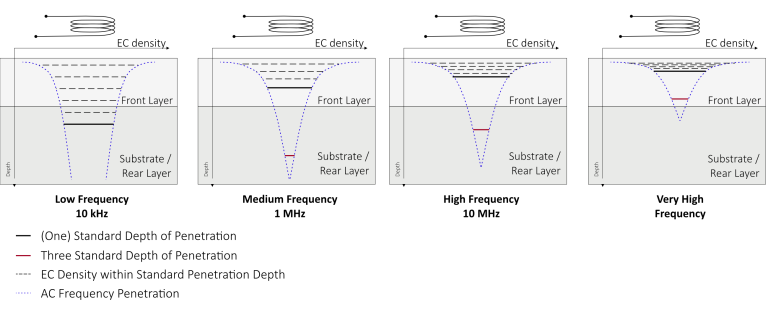
Similar to 4PP, the eddy current method is also able to determine the resistivity if thickness of the specimen is larger than the penetration depth of the induced currents. The key difference is that the penetration depth of the currents is much smaller than with 4PP setups even if one would use very small tip distances. The penetration depth, meaning the analyzing area for resistivity measurement depends on several factors. The depth of the eddy currents penetrating into a material is affected by the frequency of the eddy currents, the electrical conductivity and magnetic permeability of the specimen. The following formula is used for its theoretical calculation.
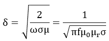
The depth of penetration decreases with increasing frequency and increasing conductivity and magnetic permeability. The depth at which eddy current density has decreased to 1/e, or about 37% of the surface density, is called the standard depth of penetration (d or 1d) and is used as criteria of ideal measurement for the investigation of bulk materials. At three standard depth of penetration (3d), the eddy current density is down to only 5% of the surface density. Further details are shown in our technology selection.
Permittivity, is known as a dielectric constant. Permittivity describes the relative ability of a dielectric to store electrostatic energy in an electric field. The smaller the relative dielectric constant of materials, the better the insulation. When a medium is applied with an electric field, the induced charge will be generated to weaken the electric field. The ratio of the original applied electric field (in vacuum) to the final electric field is called permittivity, which is also related to the frequency.
Resistivity of Semiconductors
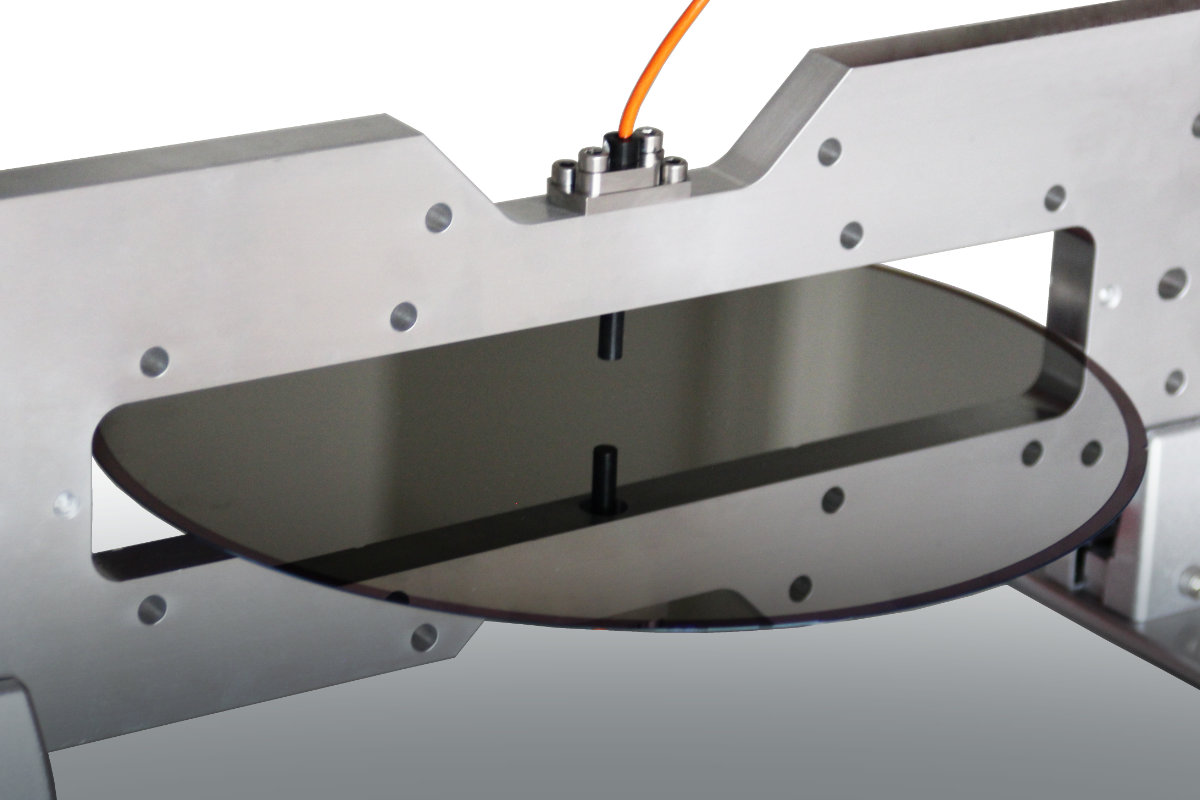
The silicon resistivity of wafer varies depending on semiconductor type and doping level, its manufacturing process and the wafer position within the ingot and also with the wafer itself. Manufacturers are trying to improve the resistivity variations from center to edge for decades. Still, resistivity variations remain which can be effectively monitored by wafer resistivity eddy current imaging. Relevant materials are mono and mono and polycrystalline wafer with p and n type doping especially in PV industry but also SiC, GaN and Si wafer or boule or ingots. Processes characterization includes growth/ creation, implantation, annealing.
Wafer Resistivity Characterization
Si Wafer can come as mono and polycrystalline materials with no doping or p and n type doping. The following graph shows the dependency of the electrical resistivity from the doping concentration of boron and phosphor / arsenic in crystalline silicon where Boron (B) doped results in n-type and Phosphor (P) / Arsenic (As) dopant to p-type semiconducting material. Eddy Current sensors are used to measure the sheet resistance of wafer, PN testers are used to determine the type of doping and capacitive sensors or optical sensors are used to determine its thickness.
SiC as material excels due to its characteristics in high temperatures, its fast switching performance and high breakdown voltage for pn junctions, which supports very compact components using higher voltages. Resistivity imaging for SiC wafers is used to detect and characterize material facets and other defects such as dislocations. The resistivity of SiC wafers can be below 1 Ohm cm ranging up to Ohm cm depending on doping level. Metallic resistivity is achieved by heavy doping with boron, aluminum or nitrogen. Superconductivity has been observed in 3C-SiC:Al, 3C-SiC:B and 6H-SiC:B at the temperature of 1.5 K. Eddy current sensors are used for wafer and boule monitoring.
GaN wafers have typical applied for LED and transistor applications. There have been great efforts worldwide to produce GaN via epitaxy processes on the widespread and inexpensive silicon wafers. Due to the strongly different lattice constants and thermal expansion coefficients of GaN and SiC, however, the applied GaN layers are challenging as they often contain defects. Resistivity imaging supports the characterization process along the processing chain.
Ingot or Block Resistivity Characterization
The resistivity within ingots varies depending on its manufacturing processes and the distribution of dopants within a wafer block or ingot. There is a center to edge and a top to bottom variation. Eddy current sensors are applied onto available surfaces for monitoring the variation. Good surface properties support a good measurement.
SiC Boule Characterization
A rather new application is the SiC boule characterization by non-contact eddy current sensors. The resistivity of SiC exposes changes in purity and grain structure. Eddy current sensors are used to analyze the SiC composition, structure, dislocation zones and to detect defected zones and assess the defect density. Additionally, electrical impedance images by high frequency eddy current sensors show the effectiveness of implantation processes and expose the quantity of subsequent annealing processes for activation of implants and show further temperature related material changes.
Graphene Characterization
Graphene as a single carbon(C) layer material has been widely investigated due to its profound electrical, mechanical and optical properties. High conductivity of graphene layer grants itself great application potential in many aspects of electronic device. Graphene’s most promising application at the moment is to become at least partially a possible replacement for silicon, making ultra-minimized transistors which will be used to produce the processors for future supercomputers, which will run hundreds of times faster due to application of graphene. There are many relevant properties of graphene layer. The sheet resistance and conductance represent not only the electrical performance but also the quality of a graphene specimens. The electrical homogeneity is great measure to characterize the performance of the manufacturing process. The non-contact SURAGUS Systems are used for measurements on various types of graphene. Their prospective sheet resistance values vary depending on scale, fabrication processes, and substrates of graphene specimen, which would be applied in different industrial fields.
Materials
A comprehensive list of materials including metals, alloys and semiconductor and their respective resistivity and conductivity can be found in our material data base.
Measurement Standards
- SEMI M87 — Test Method for Contactless Resistivity Measurement of Semi-Insulating Semiconductors
- SEMI MF673 — Test Method for Measuring Resistivity of Semiconductor Wafers or Sheet Resistance of Semiconductor Films with a Noncontact Eddy-Current Gauge
- ASTM F84-02 – Standard Test Method for Measuring Resistivity of Silicon Wafers With an In-Line Four-Point Probe (Withdrawn 2003 with no replacement)
Types of Devices for Resistivity Measurement
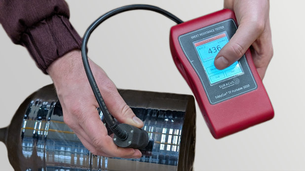
Handheld Devices
for Single Point Measurements
Handheld eddy current devices are designed for fast, random sampling of product quality—commonly used at goods receipt or for inspecting particularly large components after production.
To perform a measurement, the device is placed on the target surface. Press the “Measure” button, and within one second, the result is displayed.
Each measurement provides a precise value at the specific point tested—offering instant, reliable feedback wherever flexibility and speed are essential.
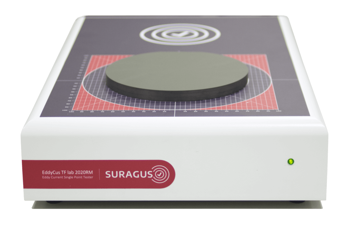
Benchtop Tools
for Single Point Measurements
Our handheld systems are ideal for quick, spot-check measurements—whether at goods receipt, during in-process inspection, or for large-format components where fixed setups are impractical.
Simply place the handheld unit on the surface to be measured, press the “Measure” button, and within one second, the measurement value appears on the display.
Each reading represents the precise value at the measurement point—giving you rapid, reliable feedback wherever you need it.
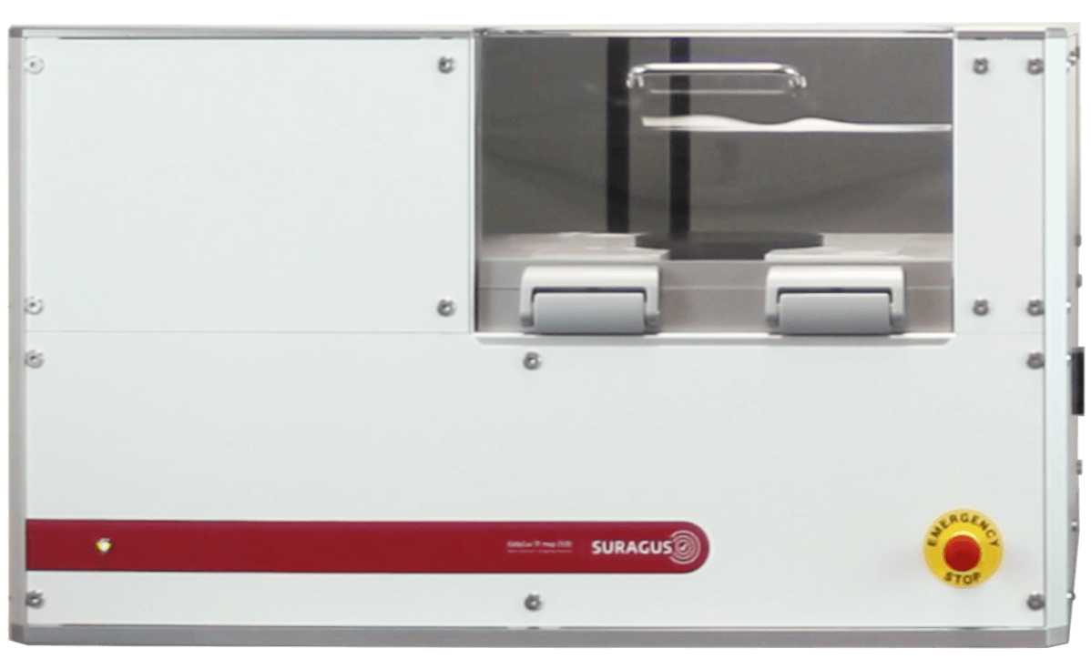
Imaging Tools
for Full Area Images
Our technology delivers highly detailed, full-surface information about product quality—enabling meaningful conclusions about process quality and stability. This data supports targeted optimization of both the manufacturing process (e.g., resource efficiency, throughput speed) and the product itself (e.g., improved homogeneity, compliance with minimum specifications).
For measurement, the sample is placed centrally on the measurement field. Prefabricated holders—such as those for wafers—ensure precise, centered positioning. Simply insert the sample, close the flap, and press “Start Measurement.”
The result: a high-resolution false-color map of the entire layer, generated from thousands of individual measurement points. This visualization gives you actionable insights at a glance.
Inline Systems
for Continuous Single Point Measurements
Our inline systems enable continuous acquisition of data on both process quality and product characteristics—before, during, or after a production step. This real-time monitoring is a foundation for production automation, which relies on precise and reliable sensor data.
The system is seamlessly integrated into your existing production line. Once the operator initiates measurement, all data is automatically recorded and stored in a centralized database.
Depending on the system configuration, the output includes one or more line profiles—either centered or positioned at critical points across the layer—providing clear insight into quality trends and process stability in real time.
Resistivity Measurement Tools
Institutes and manufacturing apply resistivity testing in very different application with very different requirement in tests per day, measurement point density and degree of automation. The following device series are available.
- Handheld
- Laboratory / Benchtop
- Single point
- Imaging
- Inline / Tool integrated