Wafer Characterization
Semiconductor wafer substrates must meet strict specifications for resistivity, homogeneity, and structural integrity before they enter device fabrication. High-frequency eddy current technology provides a fast, contact-free method for characterizing bare and processed wafers — delivering the data needed to qualify incoming material, monitor crystal growth and wafering processes, and ensure substrate quality at every stage of the supply chain.
Testing Options in Wafer Characterization
Sheet Resistance
Wafer Resistivity
Wafer Thickness
Wafer Homogeneity
Permeability
Defectoscopy
Facette Formation
Wafer Bow & Warp
Electrical Anisotropy
Applications for Wafer Characterization
Incoming Wafer Inspection
Before wafers enter device fabrication, incoming inspection verifies that the substrate material meets the required resistivity range, thickness tolerance, and homogeneity specifications. Eddy current measurement performs this check rapidly and without risk of surface damage, catching out-of-spec wafers before costly processing begins.
Wafer Imaging & Near Edge Monitoring
Wafer Process Monitoring
Wafer Quality Control
Wafer Deposition Process Control
Pre- and Post-Treatment Process Control
Typical Wafer Substrates
Silicon (Si)
| Diameter | Typical Thickness | Resistivity Range | Typical Applications |
|---|---|---|---|
| 100 mm (4″) | 525 ± 25 µm | 0.001 – 100 Ω·cm | MEMS, R&D, sensors |
| 150 mm (6″) | 675 ± 25 µm | 0.001 – 10,000 Ω·cm | Power devices, RF (FZ) |
| 200 mm (8″) | 725 ± 25 µm | 0.005 – 100 Ω·cm | IC, analog, MEMS |
| 300 mm (12″) | 775 ± 25 µm | 0.005 – 50 Ω·cm | Advanced logic, memory |
Silicon Carbide (SiC)
| Diameter | Typical Thickness | Resistivity Range | Typical Applications |
|---|---|---|---|
| 100 mm (4″) | 350 ± 25 µm | 0.01 – 0.05 Ω·cm (n-type) | R&D, legacy power devices |
| 150 mm (6″) | 350 ± 25 µm | 0.01 – 0.05 Ω·cm (n-type) | SiC MOSFETs, diodes, EV inverters |
| 150 mm (6″) | 500 ± 25 µm | > 10⁵ Ω·cm (semi-insulating) | RF, microwave, 5G |
| 200 mm (8″) | 525 ± 25 µm | 0.01 – 0.05 Ω·cm (n-type) | Next-gen power electronics |
Gallium Nitride (GaN)
| Substrate Type | Typical Diameter | Typical Thickness | Resistivity Range |
|---|---|---|---|
| Native GaN (free-standing) | 50 – 100 mm | 350 – 400 µm | 0.01 – 0.05 Ω·cm (n-type) |
| GaN-on-Si | 150 – 200 mm | 675 – 1,150 µm | Depends on Si carrier |
| GaN-on-SiC | 100 – 150 mm | 350 – 500 µm | Semi-insulating SiC carrier |
| GaN-on-Sapphire | 50 – 150 mm | 330 – 650 µm | Insulating carrier |
Sapphire (Al₂O₃)
| Diameter | Typical Thickness | Resistivity | Typical Applications |
|---|---|---|---|
| 50.8 mm (2″) | 330 ± 25 µm | Insulating (> 10¹¹ Ω·cm) | R&D, small-format LEDs |
| 100 mm (4″) | 500 – 650 µm | Insulating | LED epitaxy, optical windows |
| 150 mm (6″) | 650 ± 25 µm | Insulating | High-volume LED production |
Wafer Characterization Across Process Steps
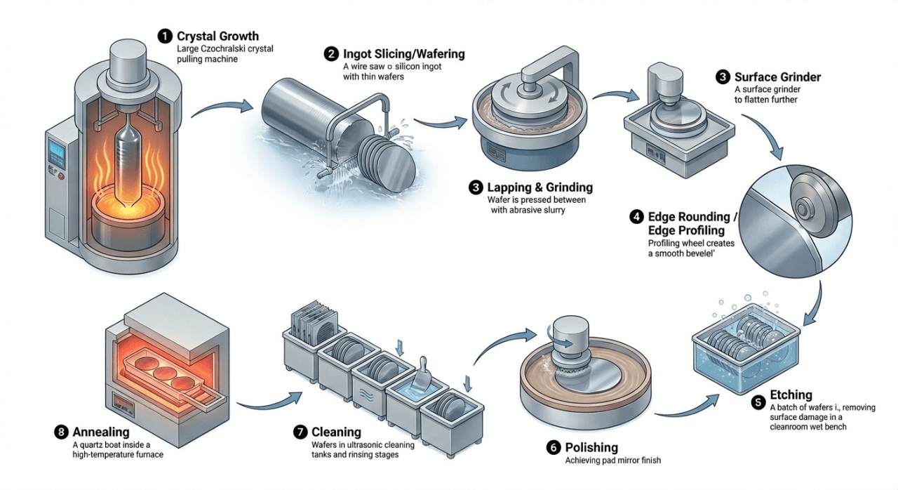
Wafer manufacturing involves a series of precisely controlled process steps — from crystal growth to final polishing. Eddy current wafer characterization can be applied between or during these steps to verify substrate quality, detect process-induced changes, and provide real-time feedback for optimization.

Crystal Growth
Ingot Slicing / Wafering
Lapping & Grinding
Edge Rounding / Edge Profiling
Edge grinding and profiling shape the wafer rim to prevent chipping and improve handling in automated equipment. While this step primarily affects geometry, eddy current near-edge measurements can verify that the edge treatment has not introduced localized resistivity changes or micro-damage in the peripheral zone of the wafer.
Etching
Chemical etching removes the remaining sub-surface damage layer left by lapping and grinding. Depending on the etchant and process parameters, etching can also affect surface resistivity and wafer geometry. Eddy current wafer characterization before and after etching quantifies the material removal and verifies that the substrate’s electrical properties remain within specification.
Polishing (CMP / SSP / DSP)
Cleaning
Annealing
Why: Qualify crystal doping & uniformity before committing to wafering
Why: Detect saw-induced variations for early sorting & grading of as-cut wafers
Why: Verify target thickness is reached & material removal is even across wafer
Why: Quantify etch removal & confirm electrical properties remain in spec
Why: Last quality gate — confirms wafer meets all specs before shipment or epitaxy
Why: Detect residual metallic contamination that cleaning may have missed
Why: Verify dopant activation & confirm target resistivity profile is achieved
Wafer Characterization Integration
Wafer Level
Batch Systems
Load Lock
Cluster Systems
Inline
Environment
Eddy current wafer characterization adapts to the full range of measurement environments encountered in semiconductor wafer manufacturing — from vacuum chambers to atmospheric offline stations.
In-Vacuo and Ex-Vacuo
In-Situ and Ex-Situ
Inline and Offline
Inline wafer characterization is embedded in the material flow and enables 100% substrate inspection in production. Offline wafer characterization is performed on sampled wafers at a dedicated station — ideal for in-depth analysis, process development, correlation studies, and customer qualification.
Wafer Characterization by Device Type
Eddy current wafer characterization supports a broad spectrum of semiconductor device segments — ensuring that the starting substrate meets the specific requirements of each end-use application.
