Different high effiency wafer based cell technologies are available in high volume manufacturing. Manufacturing costs are crucial for cells and modules. For achieving highest efficiency at lowest manfacturing cost, the following deposition processes have to be monitored:
Metal grid
Electrodes
Buffer or seed layer
Tunnel oxide
Passivation layer
Testing
Sheet resistance
Conductivity
Thickness
Homogeneity
Defectoscopy
Applications
Incoming inspection
Wafer testing
Deposition process control
Quality control
Final inspection
Substrates
n-type Si
p-type Si
Process
Inline
Carrier
Environment
In-vacuo and ex-vacuo
In-situ and ex-situ
Inline and offline
Types
HJT/ HIT
PERC/ PERT
TopCon
IBC
Tandem
Perovskite-HJT-Tandem
Use Case Wafer Incoming Inspection
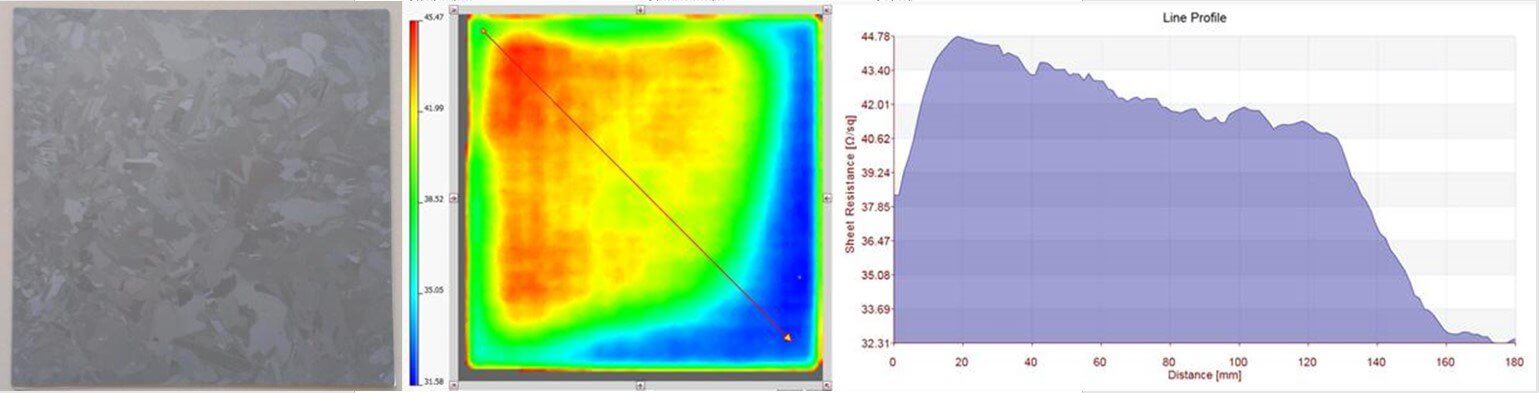
Wafer incoming inspection for poly or mono Si wafer is dedicated to sheet resistance characterization by means of high frequency eddy current technology. Measurement tasks could be realized by individual sheet resitastance characteriztation or combined with thickness measurement.
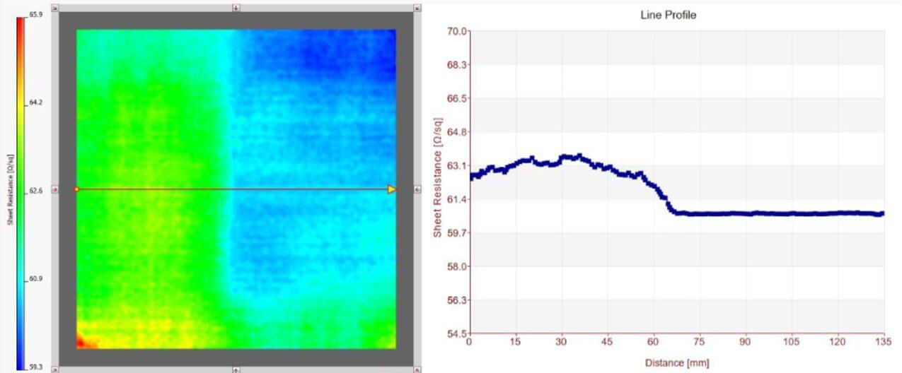
Use Case Passivation
Passivation of wafer for minimizing recombination effects can be monitored by inductive methodes such as hogh frequency eddy current technology.