Non-contact Sheet Resistance and
Metal Layer Thickness Measurement Device for Single Point Measurements
Higher thin-film and substrate quality through fast and precise laboratory devices based on non-contact eddy current technology.
- Non-contact real time measurement
- Precise measurement of conductive thin films
- Characterization of hidden and encapsulated conductive layers
- Measurement data saving and export functions
Introduction
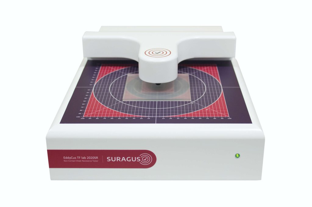
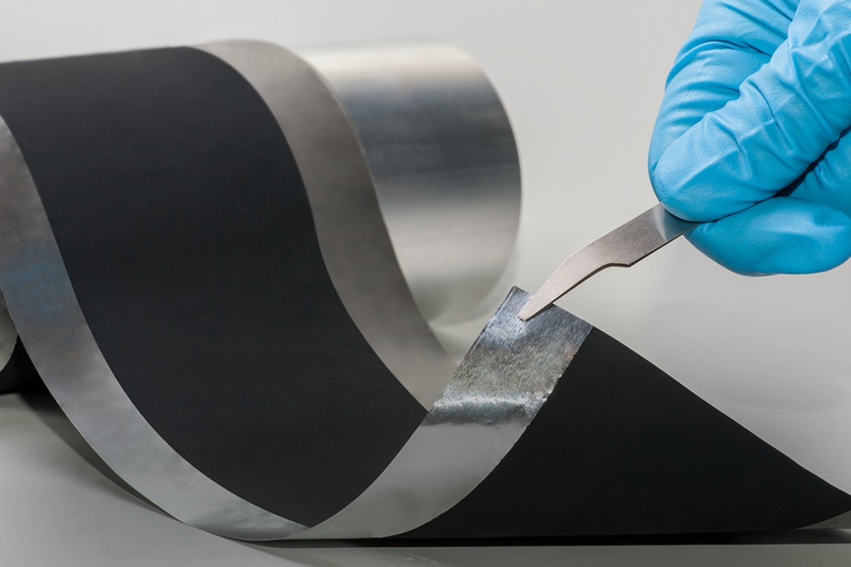
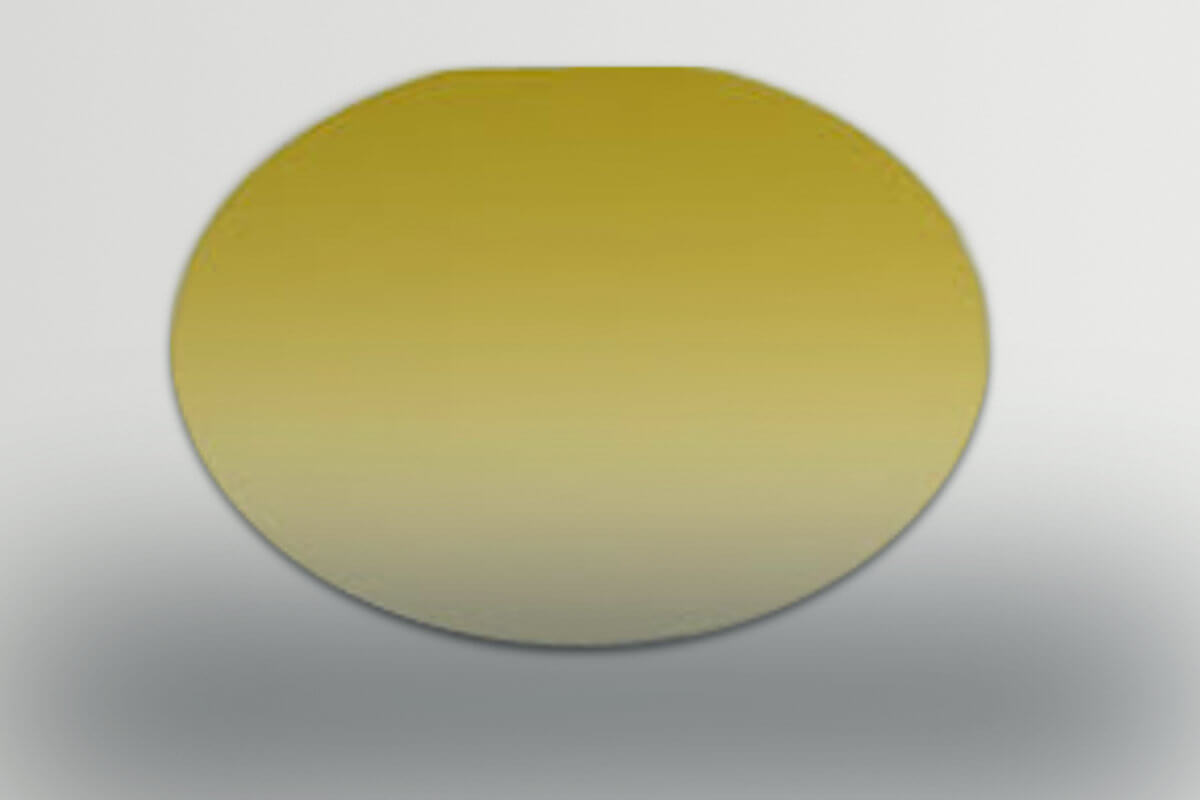
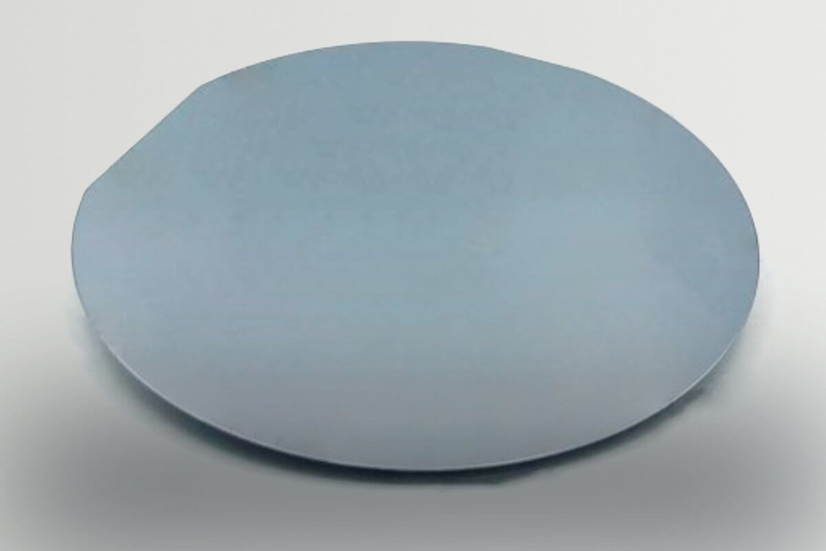
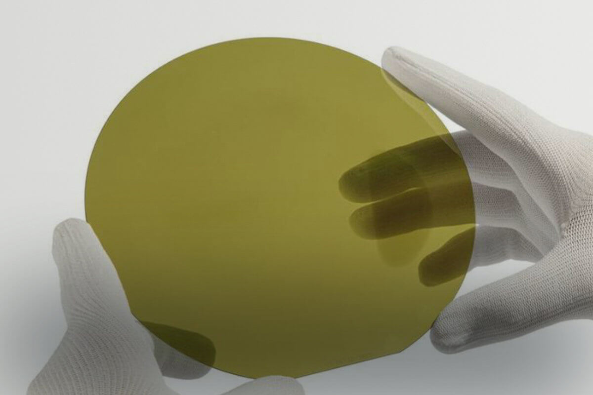
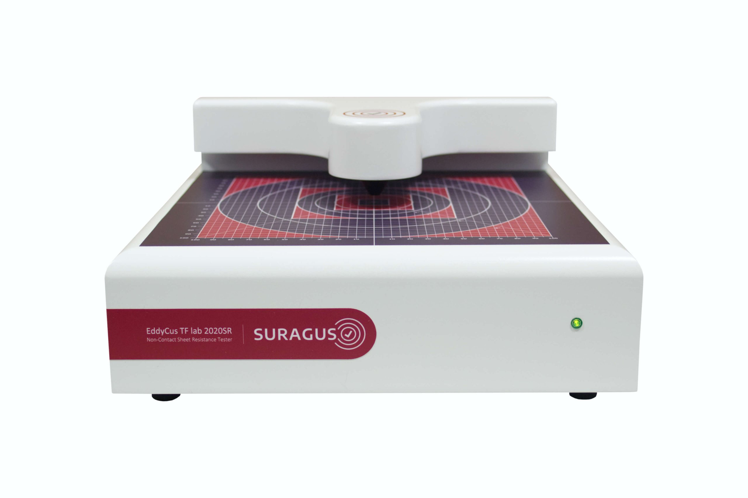
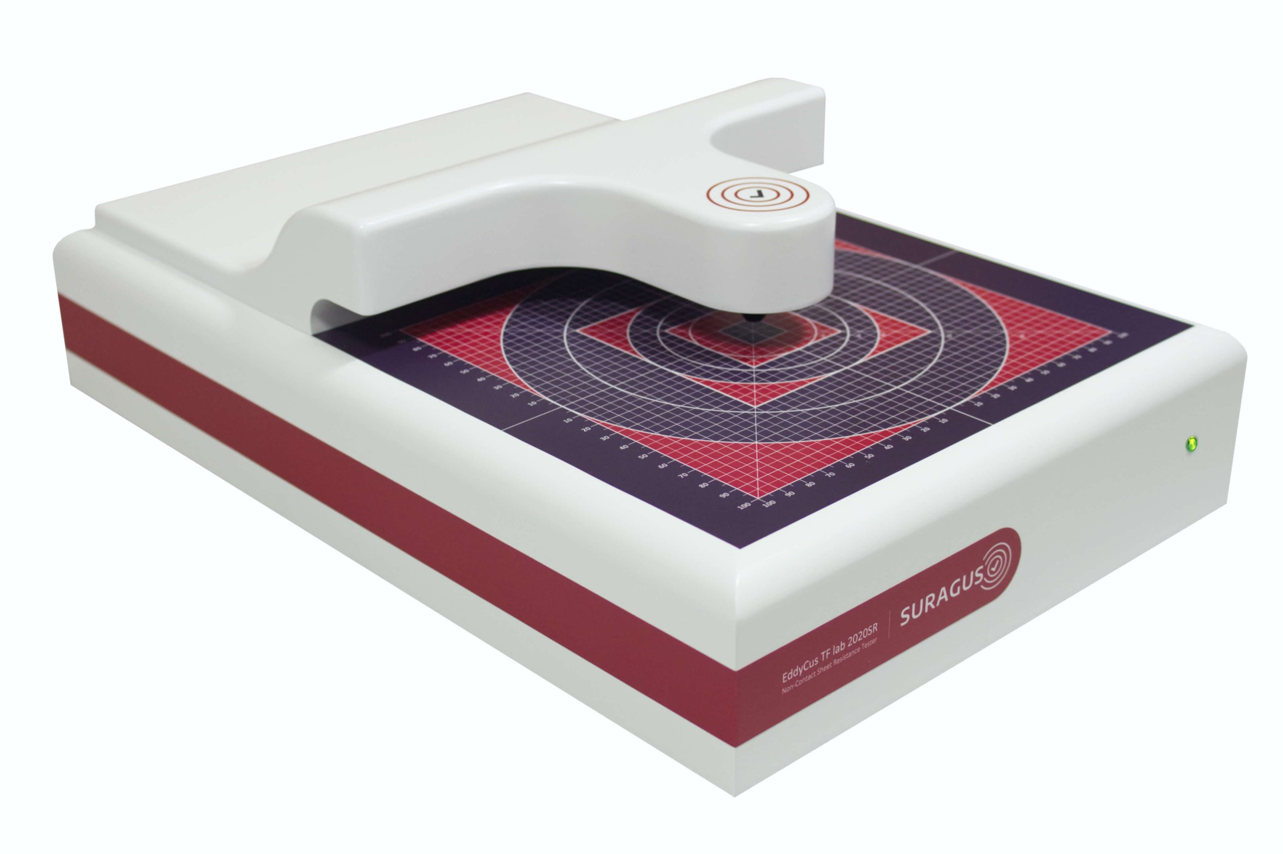
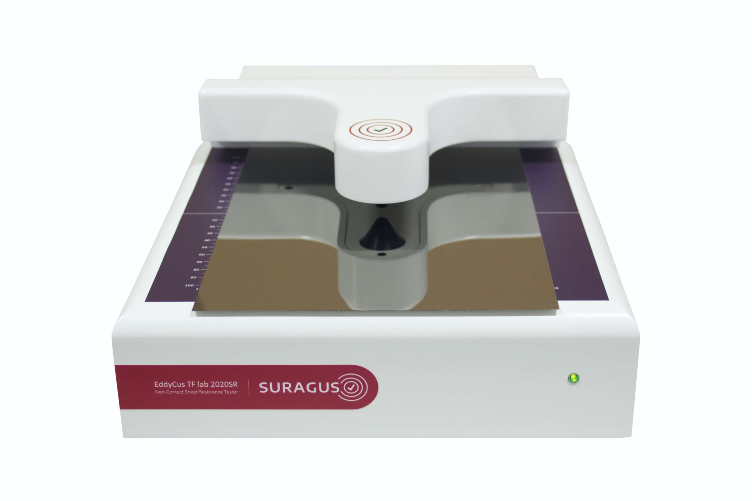
The EddyCus® lab 2020 TM Series is a compact, benchtop system designed for non-contact, single-point measurements of conductive thin films, metal layer thicknesses, and sheet resistance using eddy current technology. It enables fast, accurate measurements of samples up to 200 x 200 mm² (8 x 8 inches) and supports a broad range of materials, including thin metal layers, doped wafers, and conductive polymers.
The EddyCus® lab 2020 offers a modern, contact-free alternative to traditional 4-point probe (4PP) and other contact-based measurement methods. Unlike 4PP systems, it requires no physical contact, no surface preparation, and is unaffected by encapsulations or surface roughness.
You can learn more about the comparison between eddy current and 4PP methods [here].
These advantages make the EddyCus® lab 2020 an excellent choice for R&D laboratories, quality control, and process monitoring, where speed, repeatability, and non-destructive testing are essential.
The device is typically used for:
- Quality control, input and output control
- R&D
- Sample sizes between 10 x 10 mm² and 200 x 200 mm² (0.5 x 0.5 inches to 8 x 8 inches)
- Measurement ranges between 0.1 mOhm/sq and 100 kOhm/sq
Sensor Capabilities
Sheet Resistance [0.0001 – 200,000 Ohm/sq]
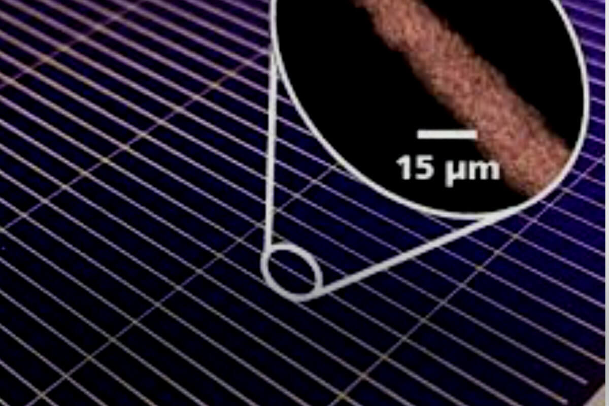
Metal Layer Thickness [1 nm – 100 µm]
Resistivity []
Electrical Anisotropy [0.33 – 3]
Sensor Gap
4 – 20 mm fixed sensor (customized upon request)
Supported Substrates
Each sample with a maximum high of 8 mm
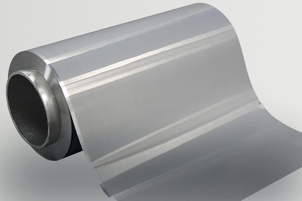
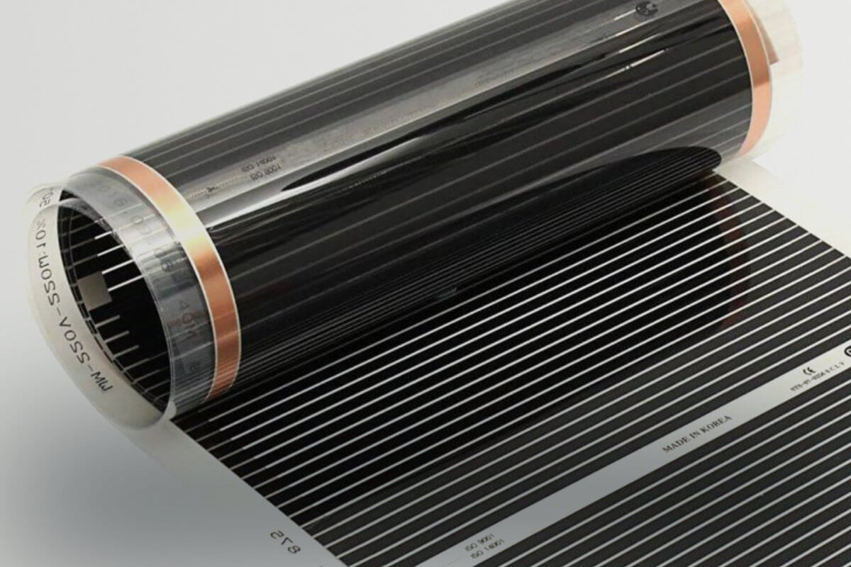
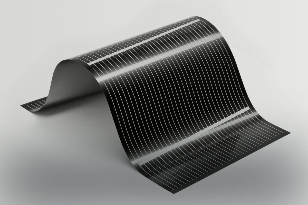
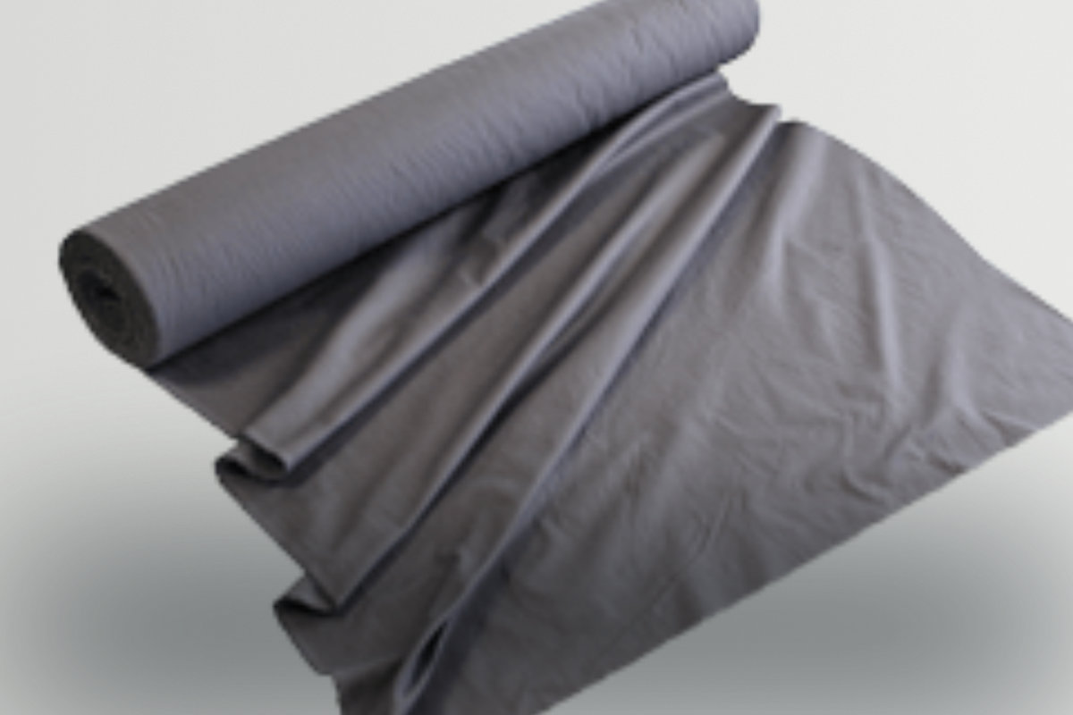
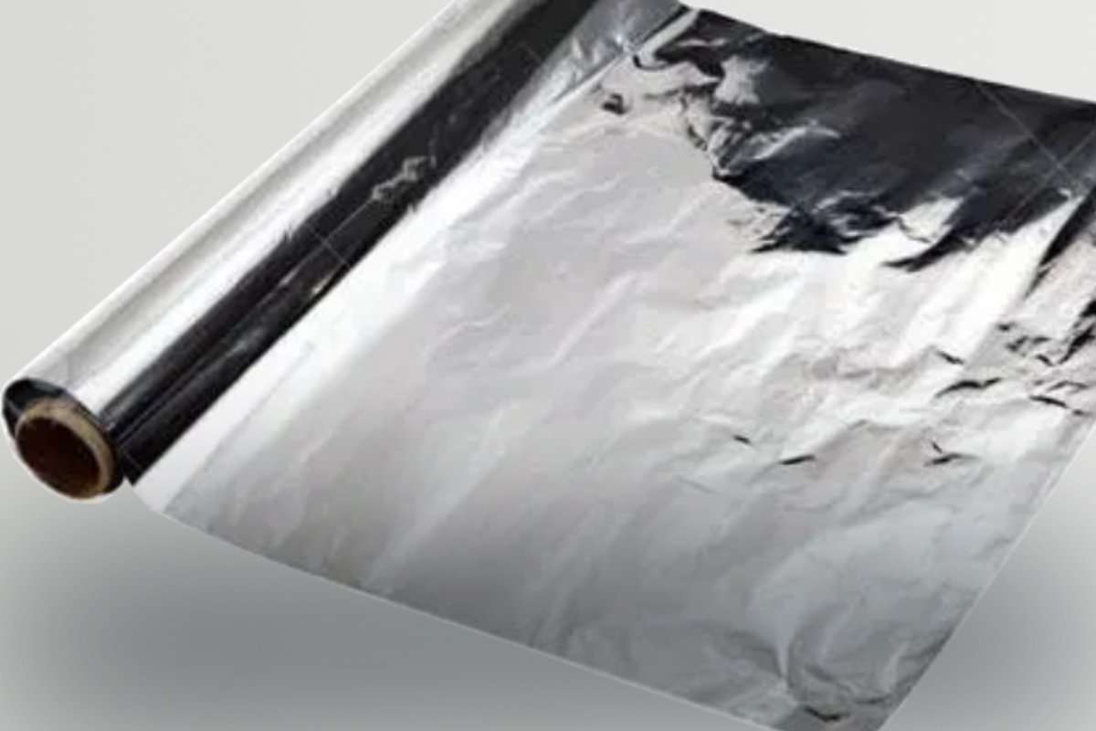
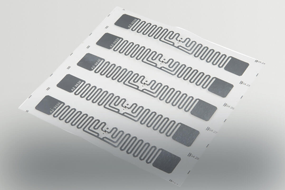
Foils, glass, wafer, solar wafer, e. g.
Measurement Field
Sample sizes between 10 mm x 10 mm and 200 mm x 200 mm.
With markings for easy positioning.
Features and Benefits
Up To 200 x 200 mm Sample Size
Wide Range of Materials
Various Analyzing Options
Instant Results
Manual Mappings
Easy to Use
3D Viewer
One Device, Multiple Measurement Parameters
The EddyCus® lab 2020 TM is capable of measuring multiple parameters. Sheet resistance correlates with metal layer thickness, emissivity, and resistivity. As long as the material properties are well known, all of these parameters can be measured with high precision.
- Sheet resistance
- Metal layer thickness
- Resistivity
- Conductivity
- Emissivity
- Electrical Anisotropy

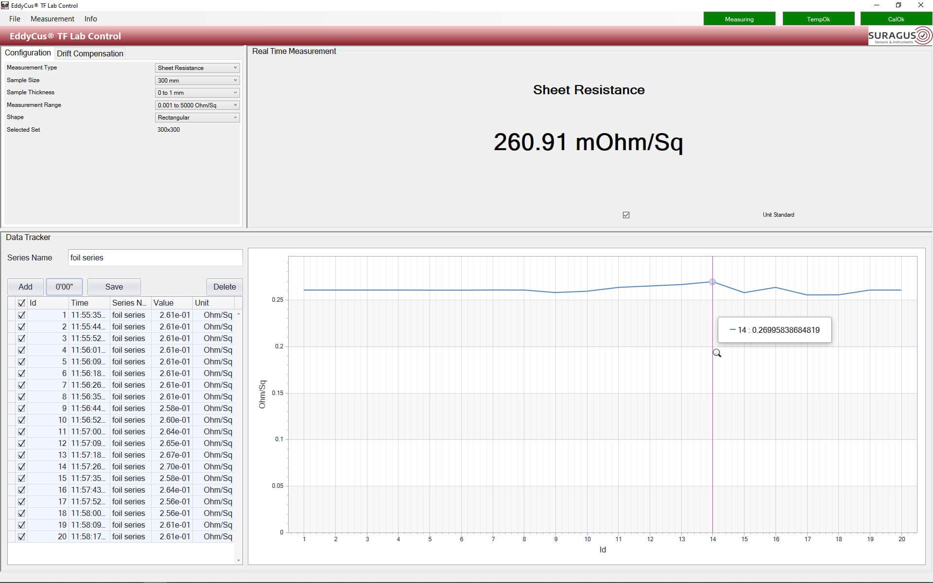
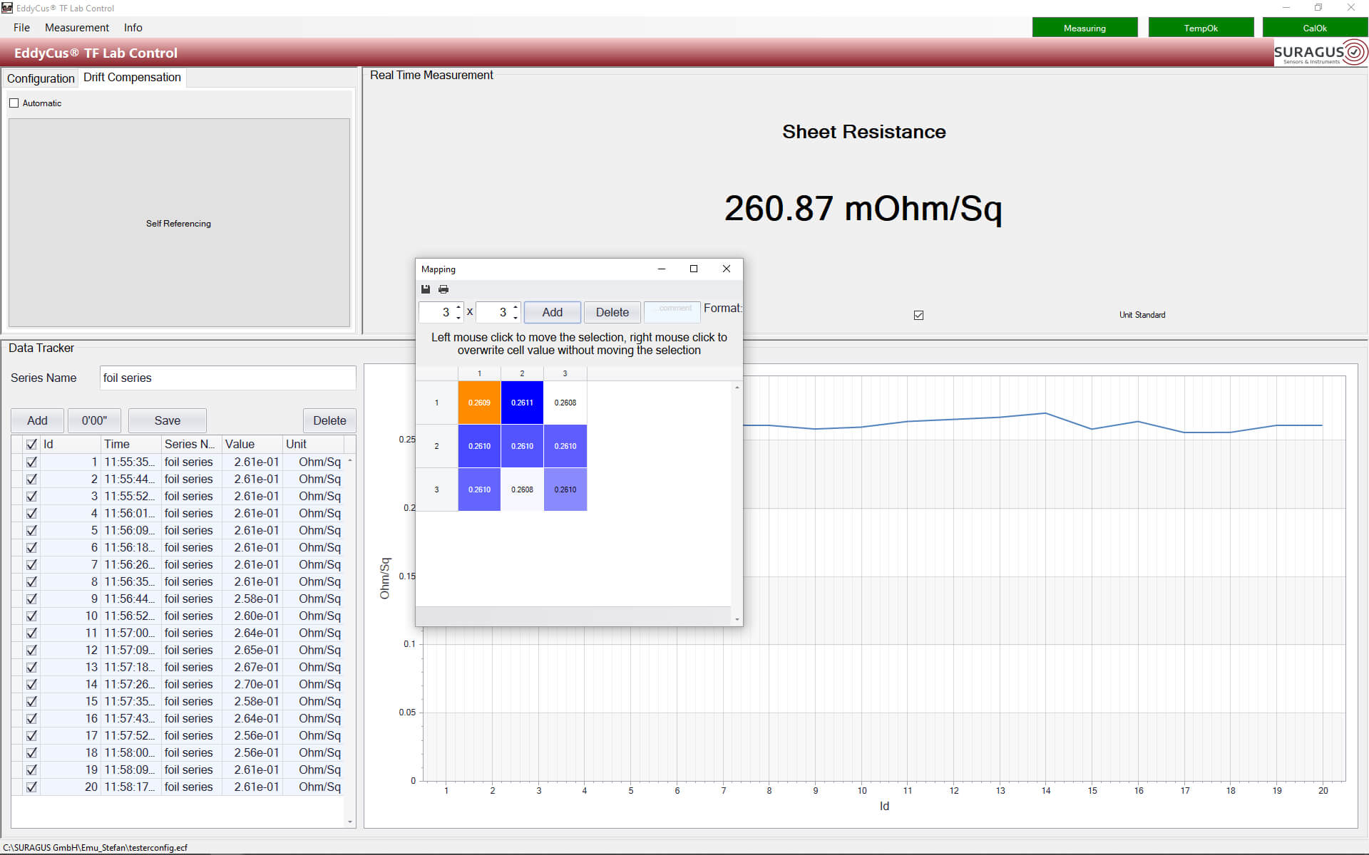

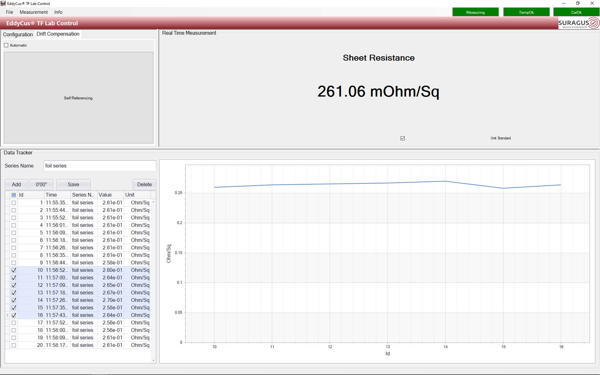
Software and Device Control
- Very user-friendly software
- Intuitive, touch display navigation
- Real-time measurement of sheet resistance and layer thickness
- Software-assisted manual mapping option
- Various data saving and export options
Video of the EddyCus® lab 2020 TM
The video gives you an impression of how to use the lab 2020 TM. Which materials can be analysed and how the device works in general.
Areas of Application
Data Table for EddyCus® lab 2020 TM
Device Features
| Measurement technology | Non-contact eddy current sensor |
| Substrates | Foils, glass, wafer, etc. |
| Substrate area | 8 inch / 204 mm x 204 mm (open on three sides) |
| Max. sample thickness / sensor gap | 3 / 5 / 10 / 25 mm (defined by the thickest sample) |
| Max. sample thickness/ sensor gap | Transmission setup: 3 – 50 mm (defined by the thickest sample) Reflection setups: infinite (only surface area is analyzed) |
| Available measurement features | Sheet resistance measurement Conductivity Resistivity Electrical anisotropy Permeability (beta) |
| Measurement range / accuracy | Depends on the measurement task, the material composition and the test object volume. Please consult the SURAGUS team |
| Device dimensions (w/h/d) | 11.4“ x 5.5” x 17.5“ / 290 mm x 140 mm x 445 mm |
| Weight | 10 kg |
Measurement Capabilities
| Sheet resistance measurement | |
|---|---|
| Sheet resistance measurement range (Five sensor setups available) |
Ultra low: 0.008 – 10 mOhm/sq; 2 – 3 % accuracy Very low: 0.05 – 300 mOhm/sq; 1 – 3 % accuracy Low: 0.001 – 100 Ohm/sq; 1 – 3 % accuracy Wide range: 0.001 – 3,000 Ohm/sq; 1 – 5 % accuracy High: 100 – 300,000 Ohm/sq; 2 – 5 % accuracy |
| Thickness measurement range of metal films (e.g. copper) | 2 nm – 2 mm (in accordance with sheet resistance (cf. our calculator)) | Metal layer thickness measurement |
| Metal thickness range Accuracies depend on the selected setup and the type / conductivity of the metal (e.g. copper, aluminum, silver) |
Low 1 – 10 nm; 2 – 5 % accuracy Standard 10 – 1,000 nm; 1 – 3 % accuracy High 1 – 100 µm; 0.5 – 3 % accuracy |
Resistivity measurement |
| Resistivity measurement range | In accordance to sheet resistance and layer thickness (cf. our calculator)) | Electrical anisotropy measurement |
| Sheet resistance range | 0.01 – 1,000 Ohm/sq; 1 to 5 % accuracy |
| Anisotropy range (TD/MD) | 0.33 – 3 (larger upon request) | Multi parameter measurement |
|
Measurement types |
Wet thickness (µm) / weight (g/m²) / drying status (%) Conductivity / resistivity (mOhm cm) / permeability (H/m) Beta Permittivity (F/m) Beta |
| Measurement range / accuracy | Depends on the measurement task, the material composition and the test object volume. Please consult the SURAGUS team |