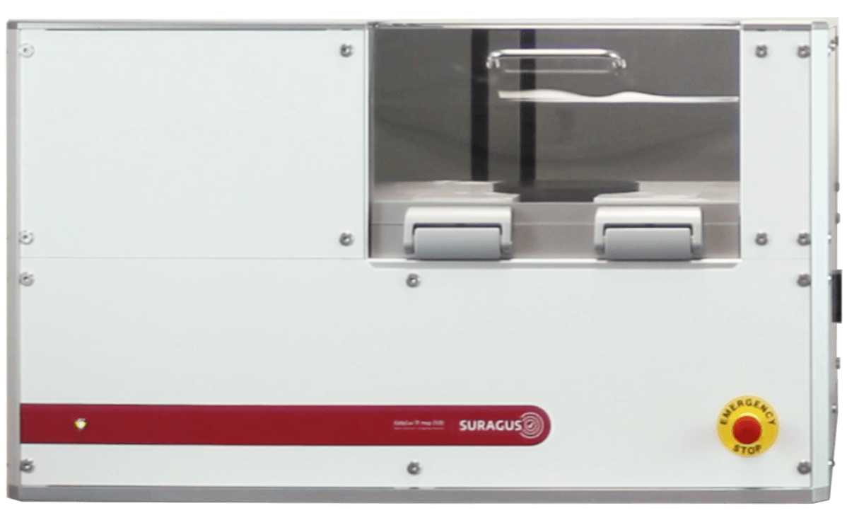
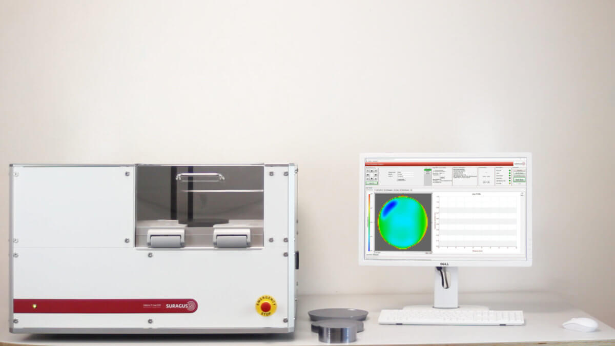
Resistvity Mapping and Defect Identification for Boules, Pucks, Ingots and Wafers
Enhanced thin-film and substrate quality through fast, precise mapping using non-contact eddy current technology. Designed for bulk materials like SiC or Si pucks up to 5 kg and 200 mm in height, with additional capability to measure wafers.
- Non-contact
- Fast and precise measurement
- High resolution mapping of conductive thin films
- Imaging of substrates up to 220 x 220 mm (8 x 8 inches)
- Characterization even of hidden and encapsulated conductive layers
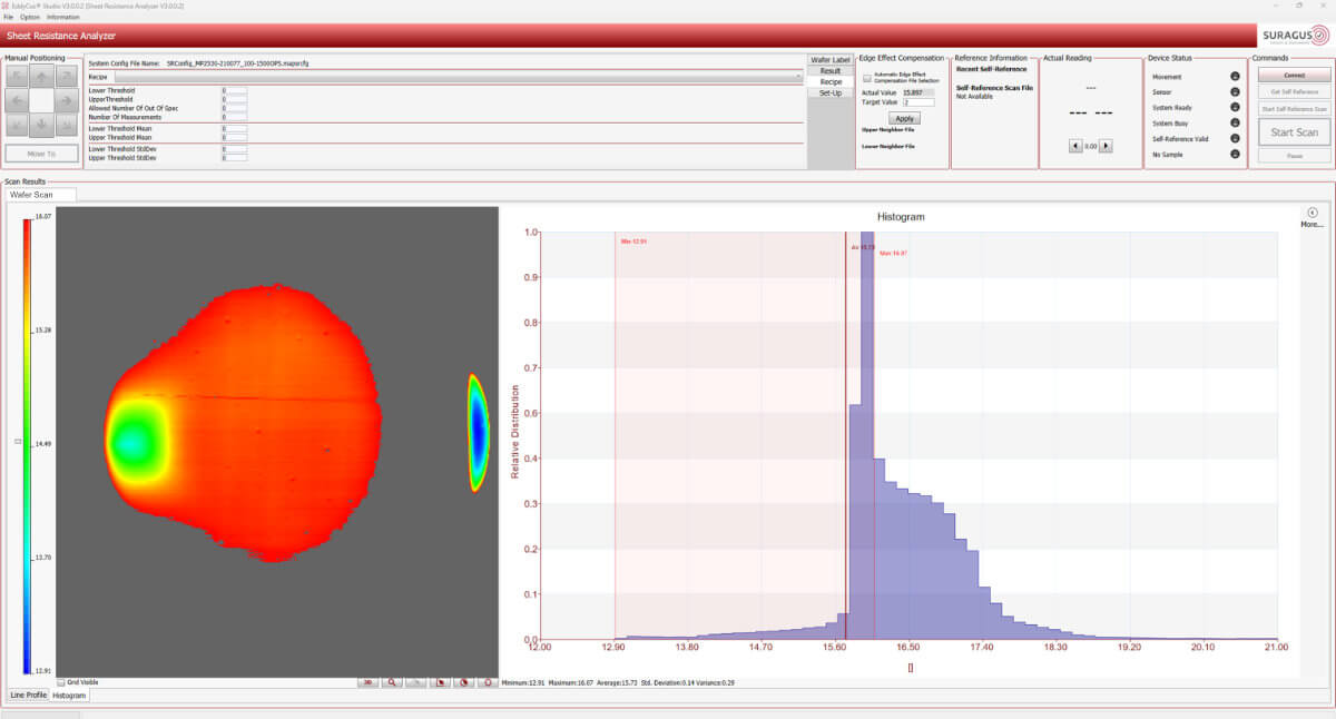
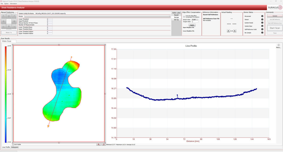
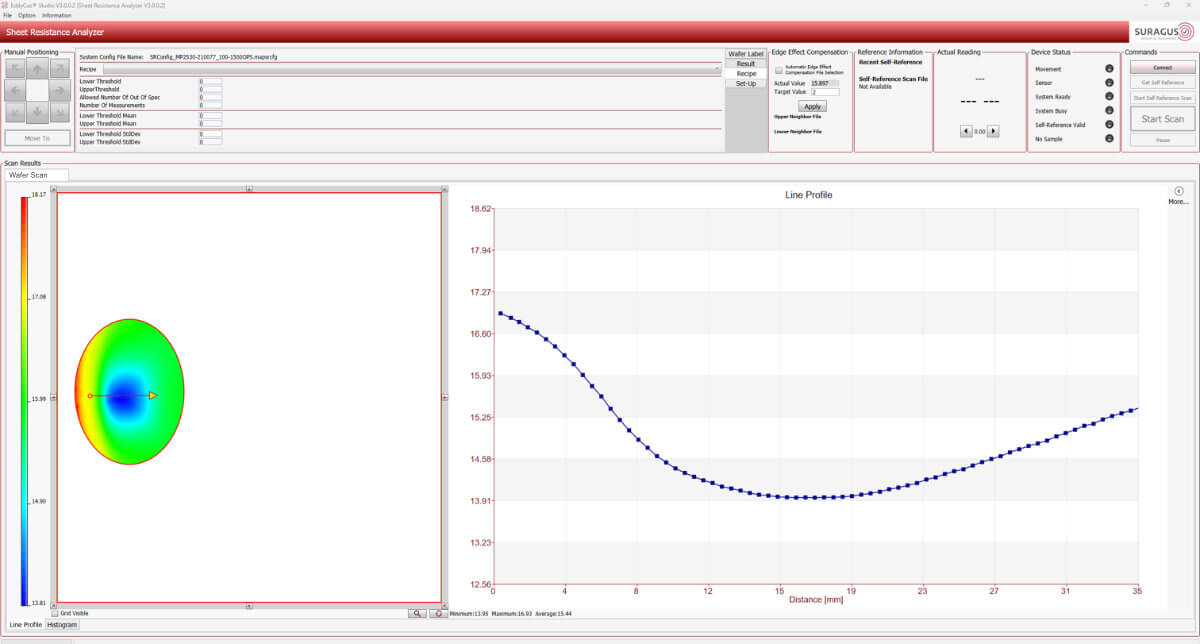
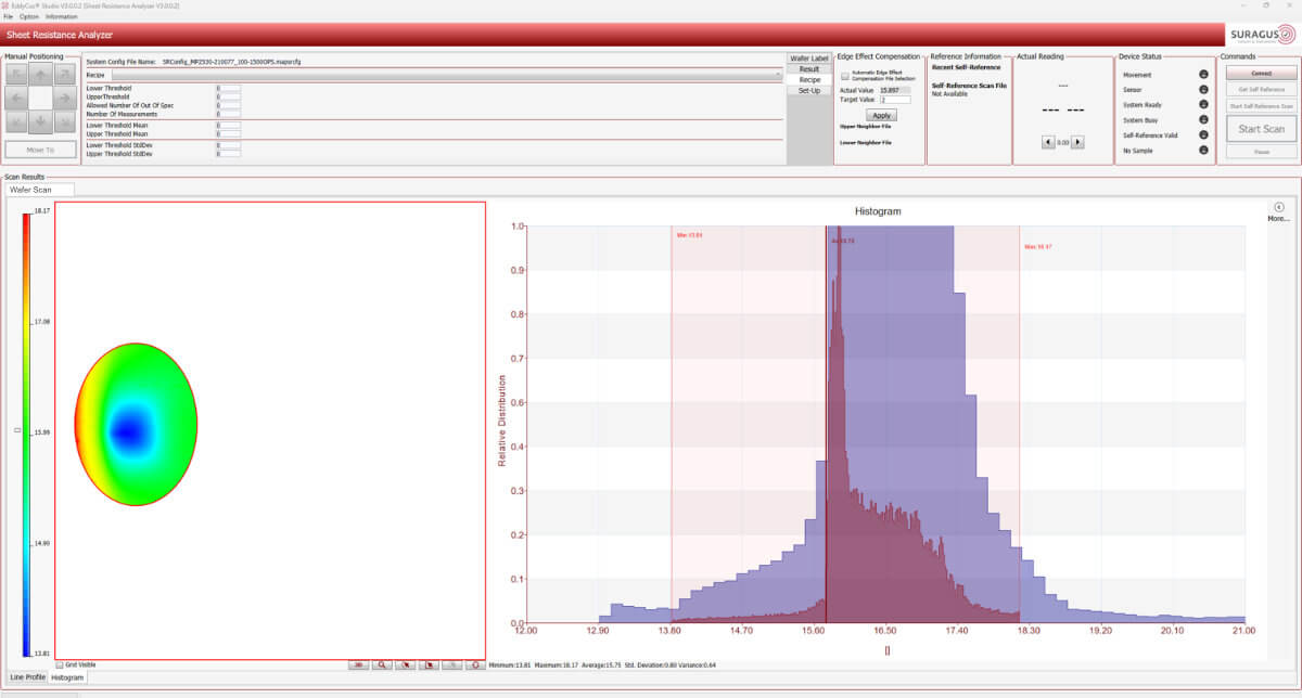
- Various software-integrated analysis functions (e.g. sheet resistance distribution, line scans, single point analysis)
- Measurement data saving and export functions
- Defect detection and coating analysis
Introduction
A variety of materials characteristics determine the conductivity of materials. Next to its composition also its structure and its purity affect the conductivity. The EddyCus® map 2530RMB is an eddy current mapping system dedicated to high-resolution imaging of conductivity and correlated characteristics exposing material properties, effects and defects. The system can be equipped with various EddyCus sensors for conductivity imaging in high resolution or high penetration and defect detection by use of differential probes. The system supports the creation of images (Eddy Current C-Scans) of the surface with a measurement pitch of 100 µm to 10 mm. The three axis systems is capable to scan 2D and 2.5D areas with a size of up to 220 x 220 mm / 8 x 8 inch. Typical applications cover the surface characterization of conductive materials such as SiC-, Graphite-, metal, alloy or steel plates or other conductive semi-finished products. Additionally, the system can be used for testing the electrical integrity of printed electronics and layers.
Eddy current testing allows the quantification of material conductivity [IACS or MS/m] or resistivity [Ohm·m]. The conductivity of materials provides information on material characteristics such as type of material and homogeneity of the material composition. Next to the direct information on electrical properties, the conductivity also contains information that relate to its thermic properties or its mechanical properties and its structural integrity.
The device is typically used for:
- Measurement range : 0.01 – 65 MS/m (0.1 – 110 % IACS)
- Specimen sizes : 50 x 50 mm to 300 x 300 mm
- Shapes: flat and curved surfaces
- Exchangeable sensors dedicated to specific measurement task
- Customized specimen holder in terms of layout and shape in favor to specimen dimensions
- Data analysis, export and reporting functions
Sensor Capabilities
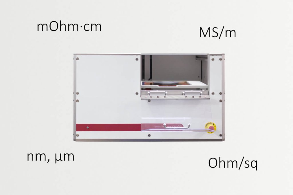
- Resistivity [0.1 – 1,000 mOhm·cm]
- Sheet Resistance [0.00005 – 100 Ohm/sq]
- Metal Layer Thickness [by conversion or direct calibration]
Supported Sample Thickness
2 – 4 mm fixed sensor (customized upon request)
Supported Substrates
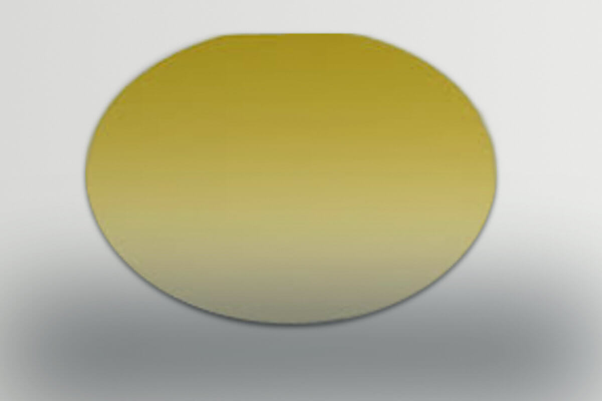
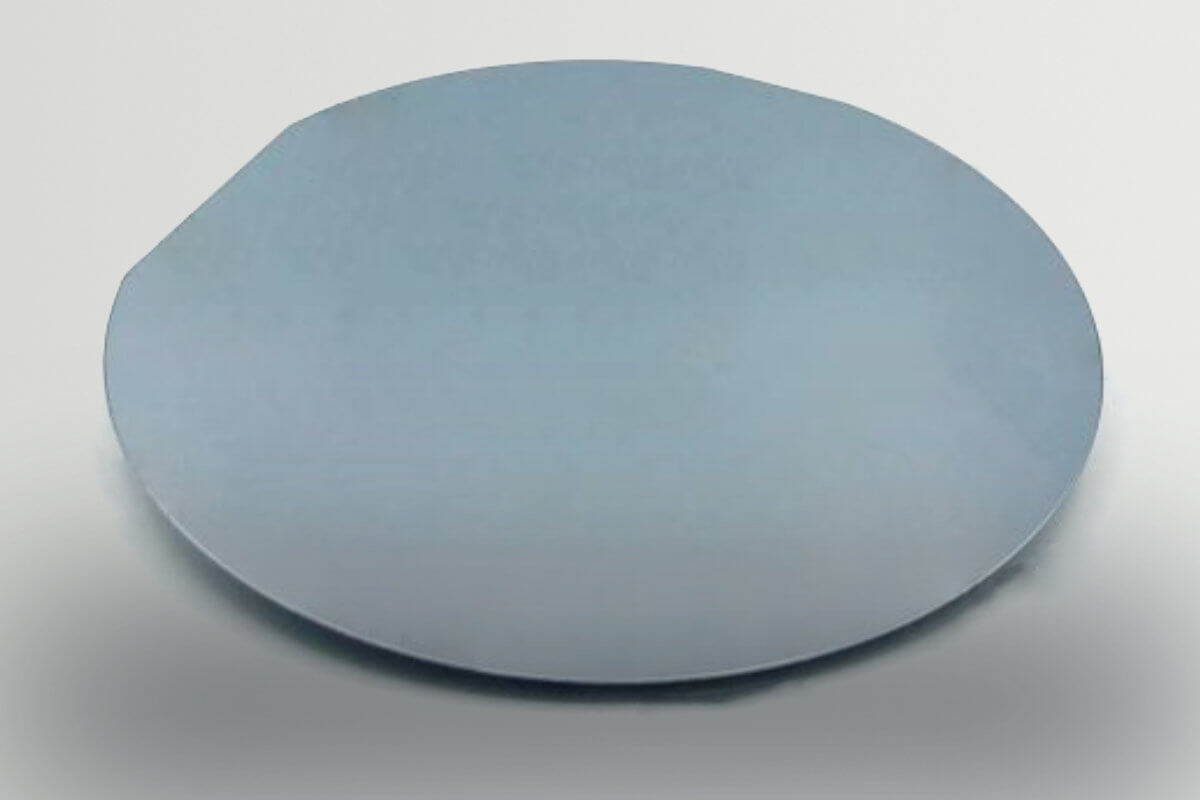
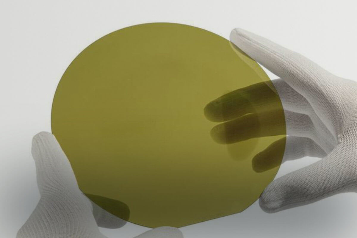
Foils, glass, wafer, solar wafer, e. g.
- Each sample with a maximum high of 200 mm
- Each sample with a maximum diameter of 300 mm
- Maximum weight 5 kg (depending on diameter)
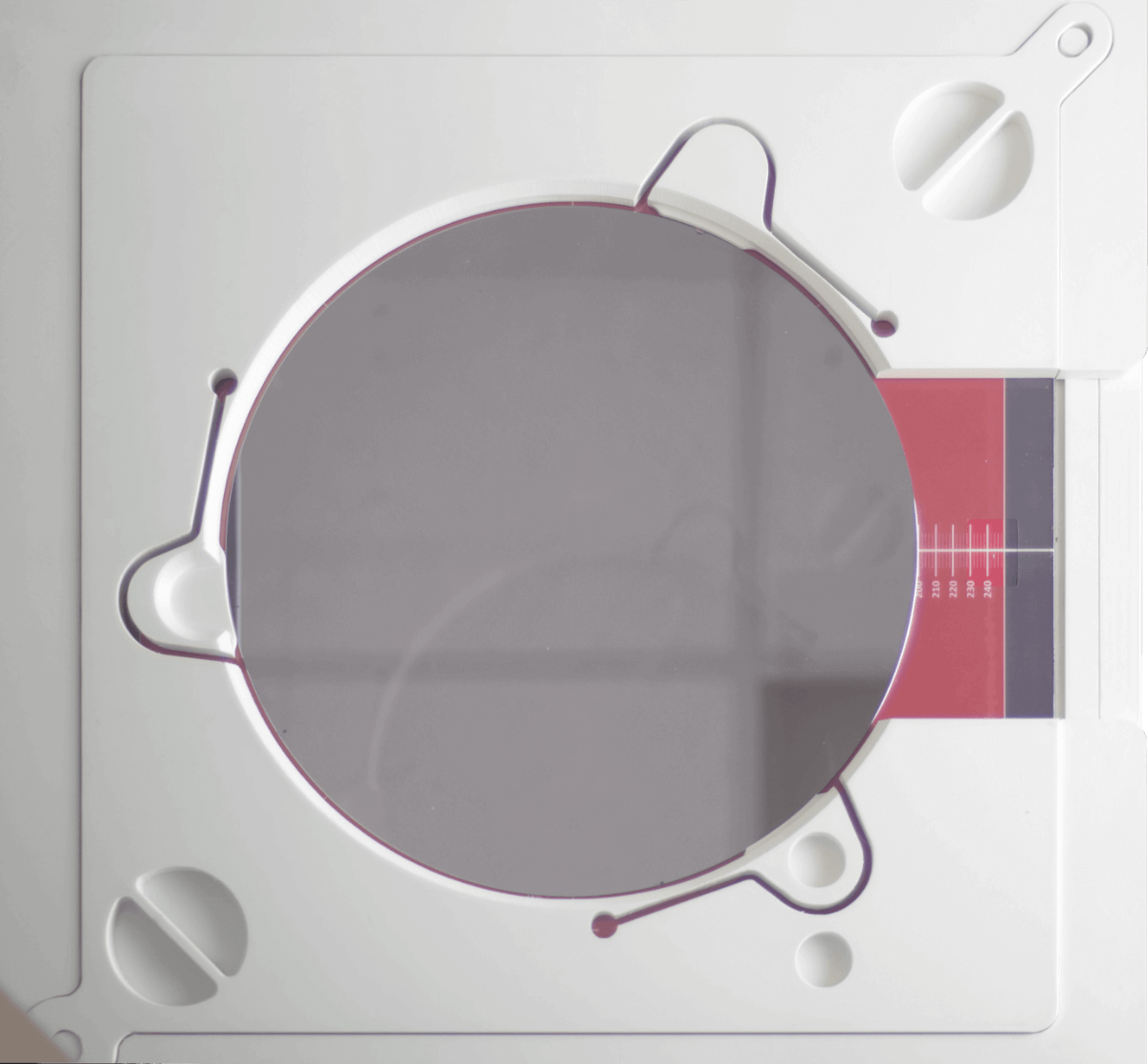
Measurement Field
- Sample sizes between 50 mm x 50 mm and 300 mm x 300 mm.
- Max. measurement area 220 mm x 220 mm
With markings for easy positioning.
Features and Benefits
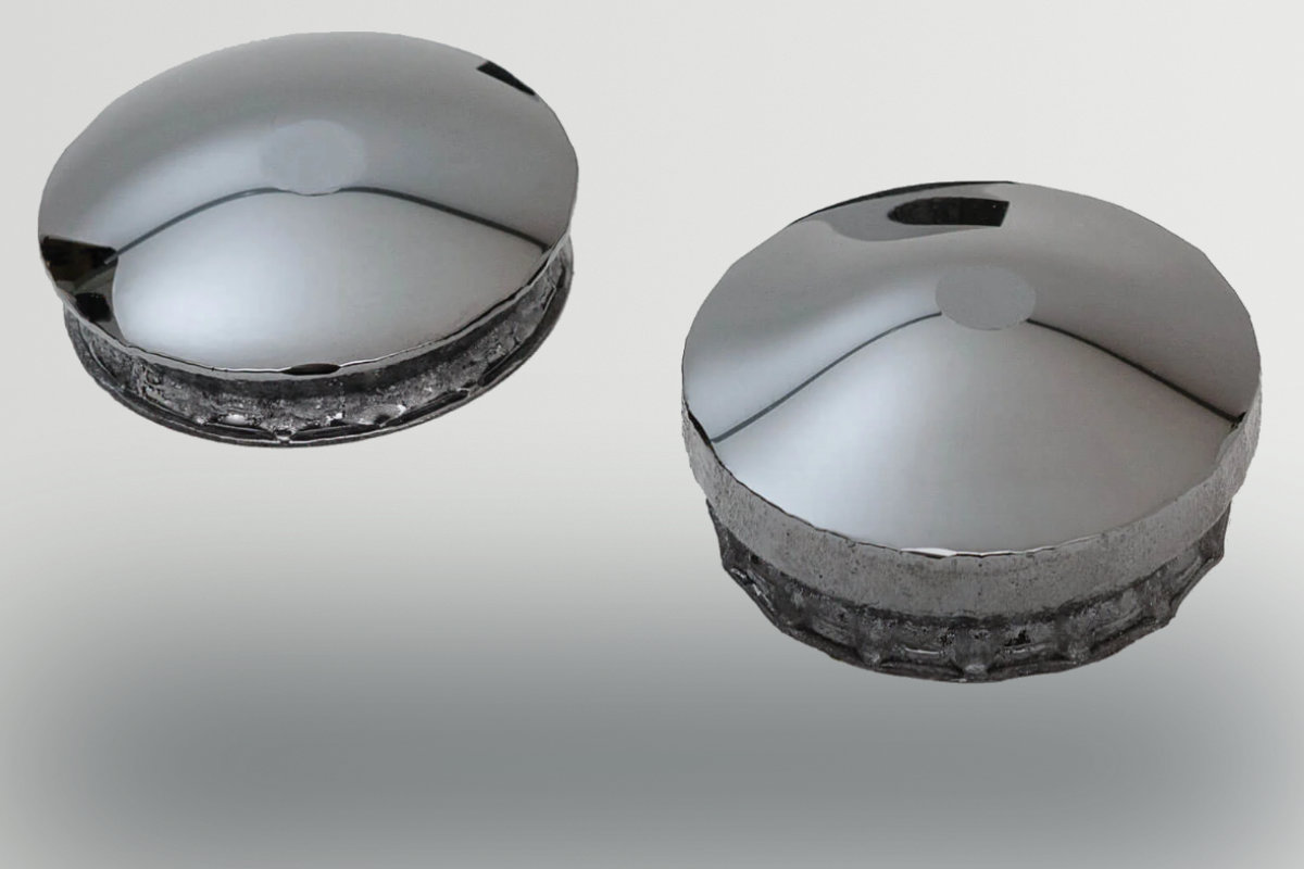
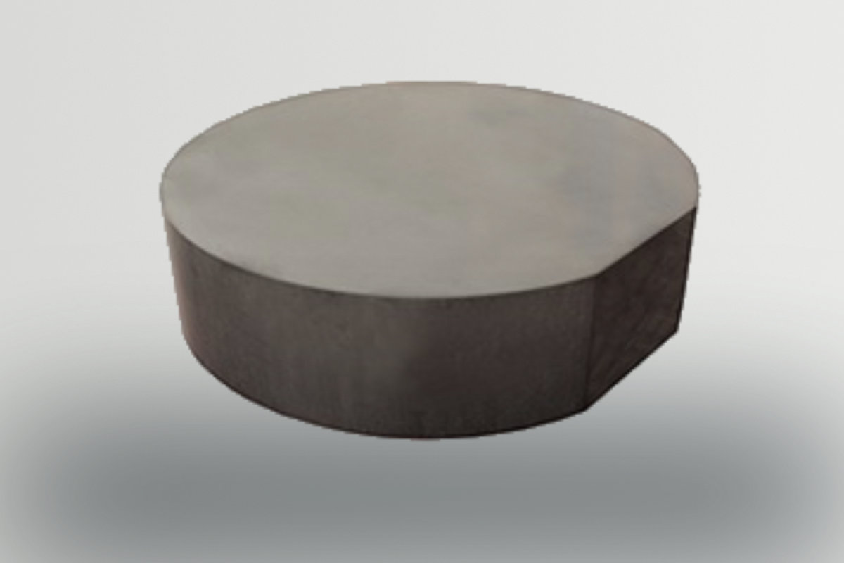
2 – 12 Inch Boules, Pucks, Ingots and Wafers
5 – 200 mm Boule, Puck, Ingot Thickness
Various Analyzing Options
Fast Results
High Resolution Mappings
Easy To Use
3D Viewer
One Device, Multiple Measurement Parameters
The EddyCus® map 2530 RMB is able to measure different measurement parameters. The resistivity correlates with sheet resistance and metal layer thickness. As long as the material is well known all of these measurement parameters can be measured precisely.
- Resistivity
- Conductivity
- Sheet resistance
- Metal layer thickness
Software and Device Control
- Very user-friendly software
- Realtime mapping measurement
- Easy-to-use statistical analysis options
- Pre-defined measurement and product recipes (sizes, pitches, thresholds)
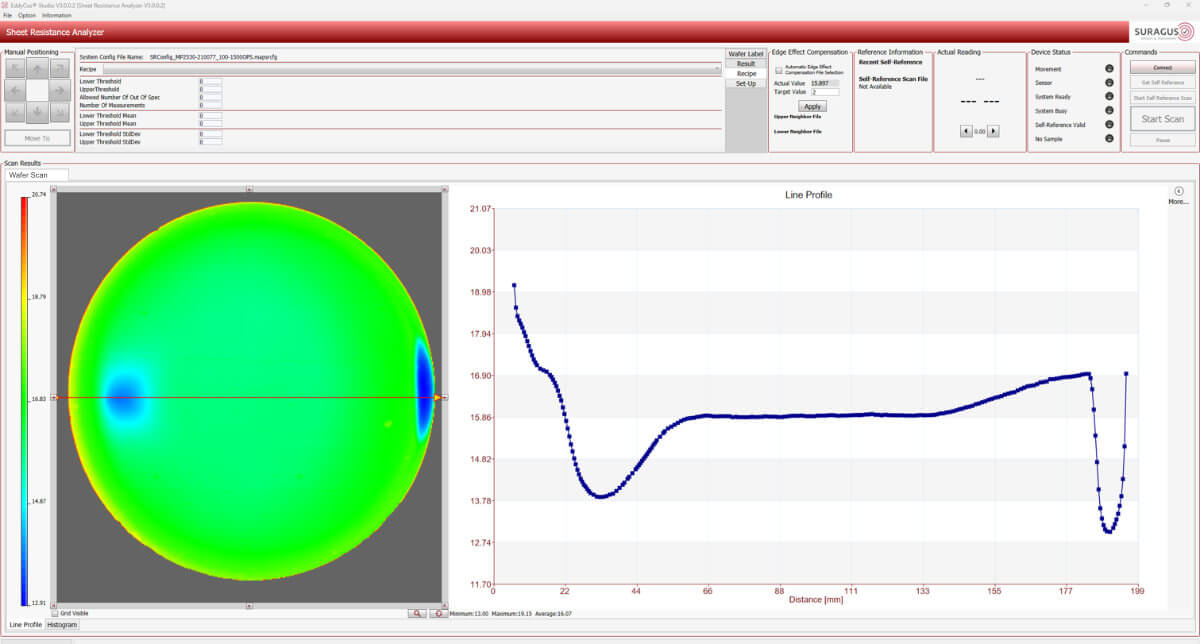
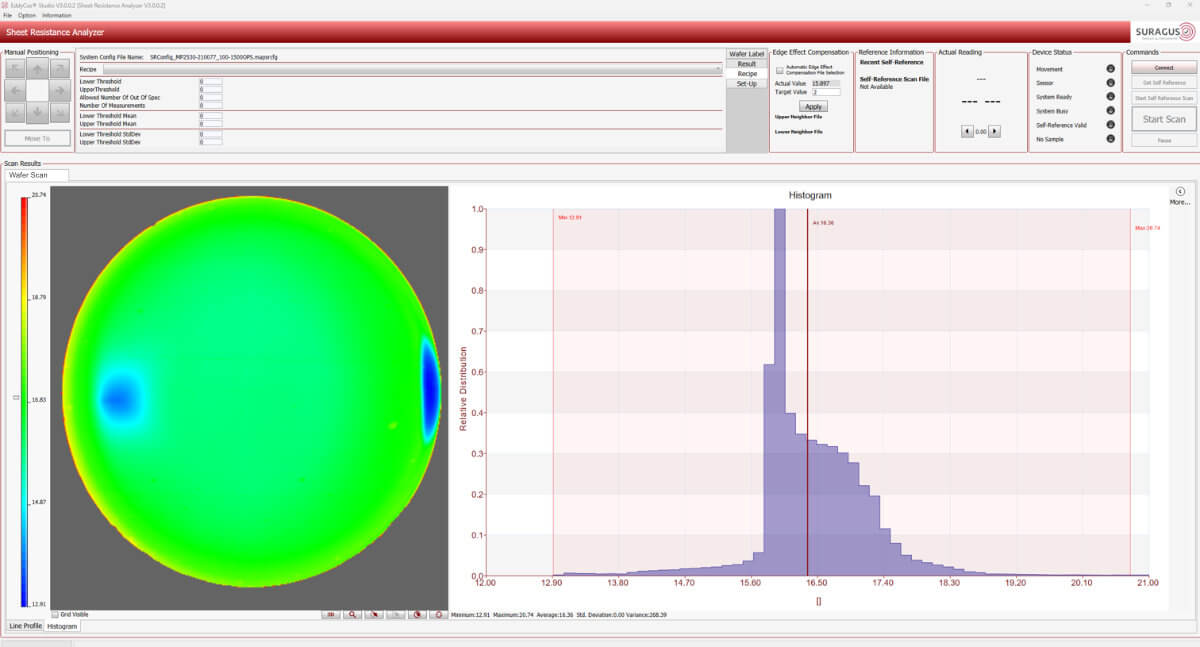
- Line scan, histogram and area analysis
- Black and colored image coding
- Csv & pdf export
- PC summary and export
- 3 user level
- Material database for parameter
- conversion
- Edge effect compensation
- Storage and import of data
- Export of data sets (e.g. to EddyEva, MS Excel, Origin)
Video of the EddyCus® map 2530 RMB
The video gives you an impression of how to use the map 2530 RMB. Which materials can be analysed and how the device works in general.
Areas of Application
Conductivity determination and conductivity imaging provides insights on:
- Material types and material purities
- Evaluation of material composition and composition variation
- Impurities/ dotation
- Variances in structure and structural integrity
- Solidification behavior of casted materials
- Conductivity-affected characteristics such as hardness, stress, grain boundaries and other characteristics
Data Table for EddyCus® map 2530 RMB
Device Features
| Measurement technology | High frequency eddy current sensor |
| Substrates | Boules, Pucks, Ingots, Wafer (Flat, slightly curved) |
| Substrate area | 12 inch / 300 mm x 300 mm (larger upon request) |
| Movement area | 8 inch / 220 mm x 220 mm (larger upon request) |
| Edge effect correction / exclusion | 2 – 10 mm (depending on size, range, setup and requirements) |
| Max. sample thickness | 200 mm (max. 5 kg) |
| Scanning pitch | 0.1 / 1 / 2.5 / 5 / 10 / 25 mm (other upon request) |
| Speed | 400 mm per second (time 1 to 30 minutes) |
| Mode | Contact and non-contact |
| Available measurement features | Resistivity imaging Conductivity imaging Sheet resistance imaging Metal thickness imaging Electrical anisotropy map |
| Device dimensions (w/h/d) | 31.5” x 19.1” x 33.5” / 785 mm x 486 mm x 850 mm |
| Weight | 90 kg |
Measurement Capabilities
| Resistivity measurement | |
|---|---|
| Resistivity measurement range |
0.1 – 1 mOhm·cm; 2 – 5 % accuracy 1 – 10 mOhm·cm; 1 – 3 % accuracy 10 – 30 mOhm·cm; 1 – 3 % accuracy 30 – 100 mOhm·cm; 1 – 3 % accuracy 100 – 1,000 mOhm·cm; 3 – 5 % accuracy |
Sheet resistance measurement |
| Sheet resistance measurement range |
0.05 – 0.1 mOhm/sq; 1 – 2 % accuracy 0.1 – 10 mOhm/sq; 1 – 2 % accuracy 10 – 100 mOhm/sq; 1 – 2 % accuracy 100 – 1,000 mOhm/sq; 1 – 2 % accuracy 1,000 – 10,000 mOhm/sq; 1 – 2 % accuracy 10,000 – 100,000 mOhm/sq; 3 – 5 % accuracy |
Metal layer thickness measurement |
|
Metal layer thickness measurement range |
Metal thickness measurement by conversion or direct calibration |