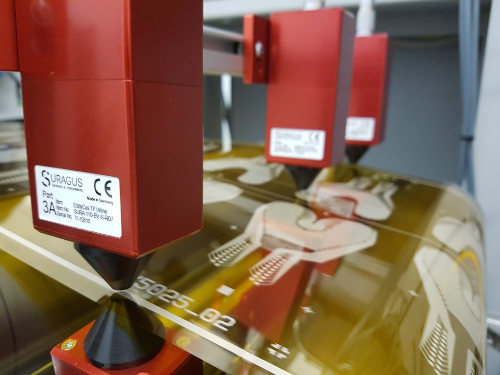
EddyCus® inline Sensorline
Full-area Sheet Resistance and Layer Thickness Measurement Solution for Process Control Higher Thin-film and substrate quality through fast and precise multi sensor Inline Measurement based on non-contact eddy current technology. Non-contact real time measurement High measurement speed up to 50 measurements/ sec. Fixed sensor installation or traversing sensor installation Integration of 1 – 99 monitoring […]
EddyCus® inline
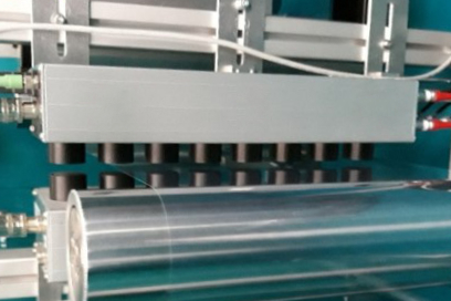
Non-Contact Process and Quality Monitoringfor Conductive Materials and Coatings highly flexible inline measurement solutions, seamlessly adaptable to your specific production process. Non-contact real time measurement High measurement speed up to 1,000 measurements/ sec. Fixed sensor installation or traversing sensor installation Integration of 1 – 99 monitoring lanes per system Process control at atmosphere or in […]
EddyCus® ResMapper
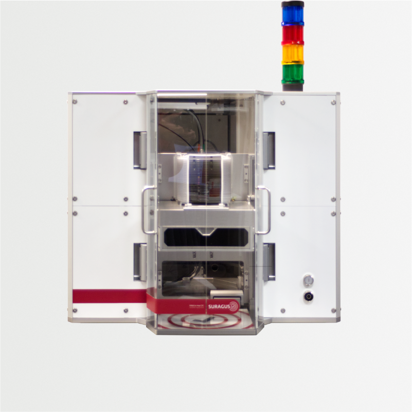
Fully Automated Wafer Imaging Device with Automated Cassette Handling System Higher Thin-film and substrate quality through fast and precise mapping devices based on non-contact eddy current technology. High resolution images with over 20 000 measurement points Up to 60 wafers per hour Measurement up to the edge of the sample All-in-one measurement of optical and […]
EddyCus® map 2530 RMT – Mixed Solutions
Multi Application Imaging Device Higher Thin-film and substrate quality through fast and precise mapping devices based on non-contact eddy current technology. High resolution images with over 30 000 measurement points within 4 minutes for best defect detection Measurement up to the edge of the sample Various analyzing options such as line profiles or histogram Various […]
EddyCus® map 2530 RMT
Resistvity Mapping and Defect Identification for Boules and Pucks Fast, precise mapping with non-contact eddy current technology improves thin-film and substrate quality. The short distance to the sample boosts signal strength and allows for a smaller spot size, enabling measurements close to the edge. High resolution images with over 30 000 measurement points within 4 […]
EddyCus® map 2530 RMB for Wafer and Metallizations
Mapping of Wafers and Metallization Layers Improved thin-film and substrate quality is achieved through high-resolution mapping enabled by non-contact eddy current technology. The EddyCus® map 2530 RMB, with its minimal spot size, allows for precise measurements in close proximity to the sample edge. Non-contact Fast and precise measurement High resolution mapping of conductive thin films […]
EddyCus® map 2530 RMB
Resistvity Mapping and Defect Identification for Boules, Pucks, Ingots and Wafers Enhanced thin-film and substrate quality through fast, precise mapping using non-contact eddy current technology. Designed for bulk materials like SiC or Si pucks up to 5 kg and 200 mm in height, with additional capability to measure wafers. Non-contact Fast and precise measurement High resolution mapping […]
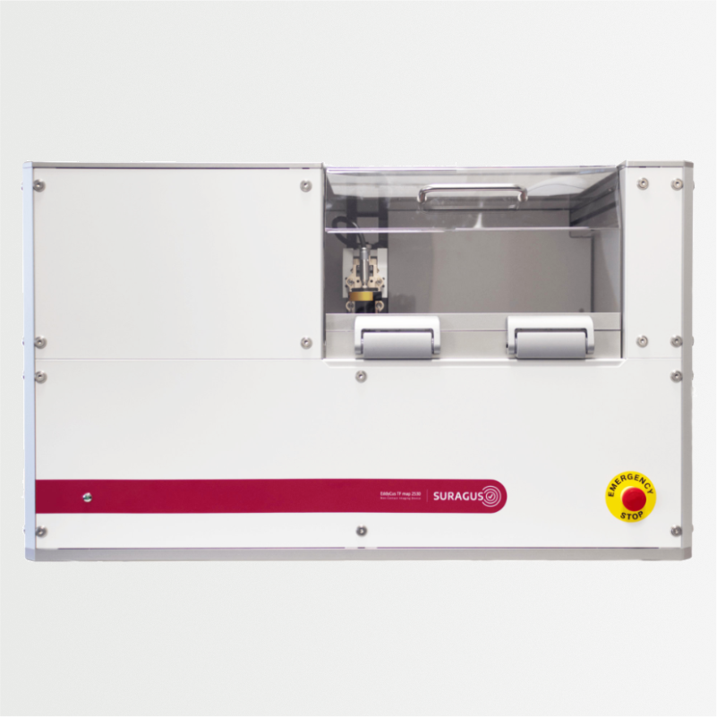
EddyCus® map 2530 TM
Non-contact Sheet Resistance and Metal Layer Thickness Mapping Device Improve thin-film and substrate quality with fast, precise, non-contact mapping. The device accurately measures sheet resistance and correlating parameters in wafers, foils, glass, and metallized layers. Non-contact Fast and precise measurement High resolution mapping of conductive thin films Imaging of substrates up to 300 x 300 […]
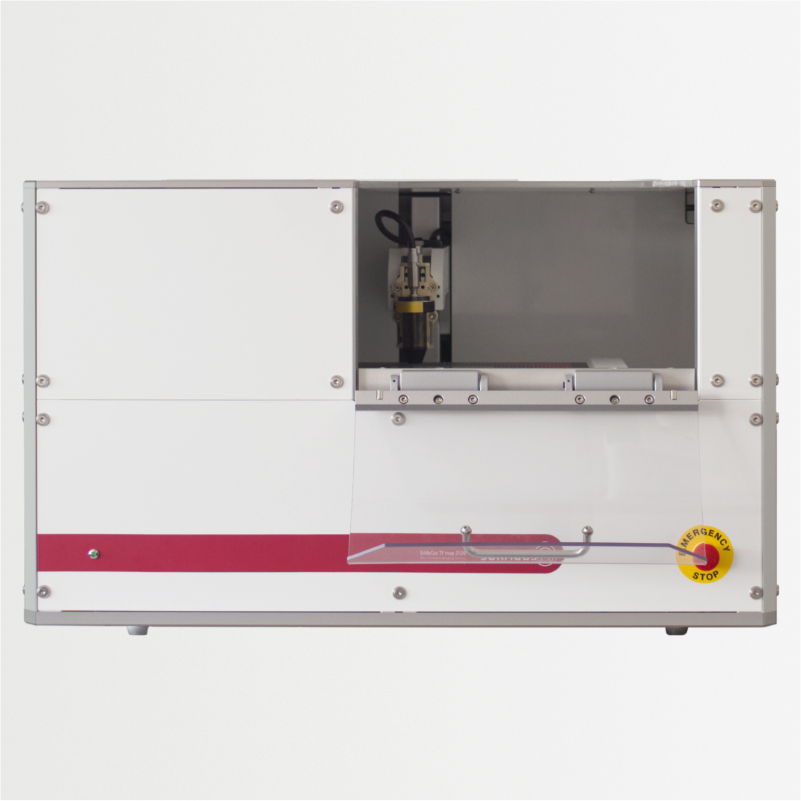
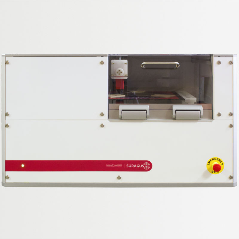
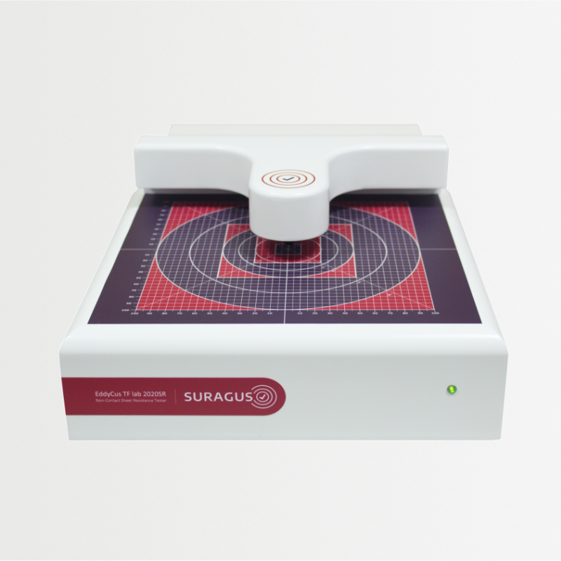
EddyCus® lab 2020 RMB
Multi-Purpose Single PointResistivity Tester Higher material and substrate quality through fast and precise laboratory devices based on non-contact eddy current technology. Non-contact real time measurement Precise measurement of conductive thin films Characterization of hidden and encapsulated conductive layers Measurement data saving and export functions Contact Us Request Demo Measurement Eddy Current Technology Download Data Sheet […]
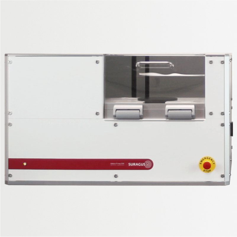
EddyCus® lab 2020 TM
Non-contact Sheet Resistance and Metal Layer Thickness Measurement Device for Single Point Measurements Higher thin-film and substrate quality through fast and precise laboratory devices based on non-contact eddy current technology. Non-contact real time measurement Precise measurement of conductive thin films Characterization of hidden and encapsulated conductive layers Measurement data saving and export functions Contact Us […]