Resistvity Mapping and Defect Identification for Boules and Pucks
Fast, precise mapping with non-contact eddy current technology improves thin-film and substrate quality. The short distance to the sample boosts signal strength and allows for a smaller spot size, enabling measurements close to the edge.
- High resolution images with over 30 000 measurement points within 4 minutes for best defect detection
- Up to 100 mm height samples with a weight up to 10 kg
- Measurement up to the edge of the sample
- Various analyzing options such as line profiles or histogram
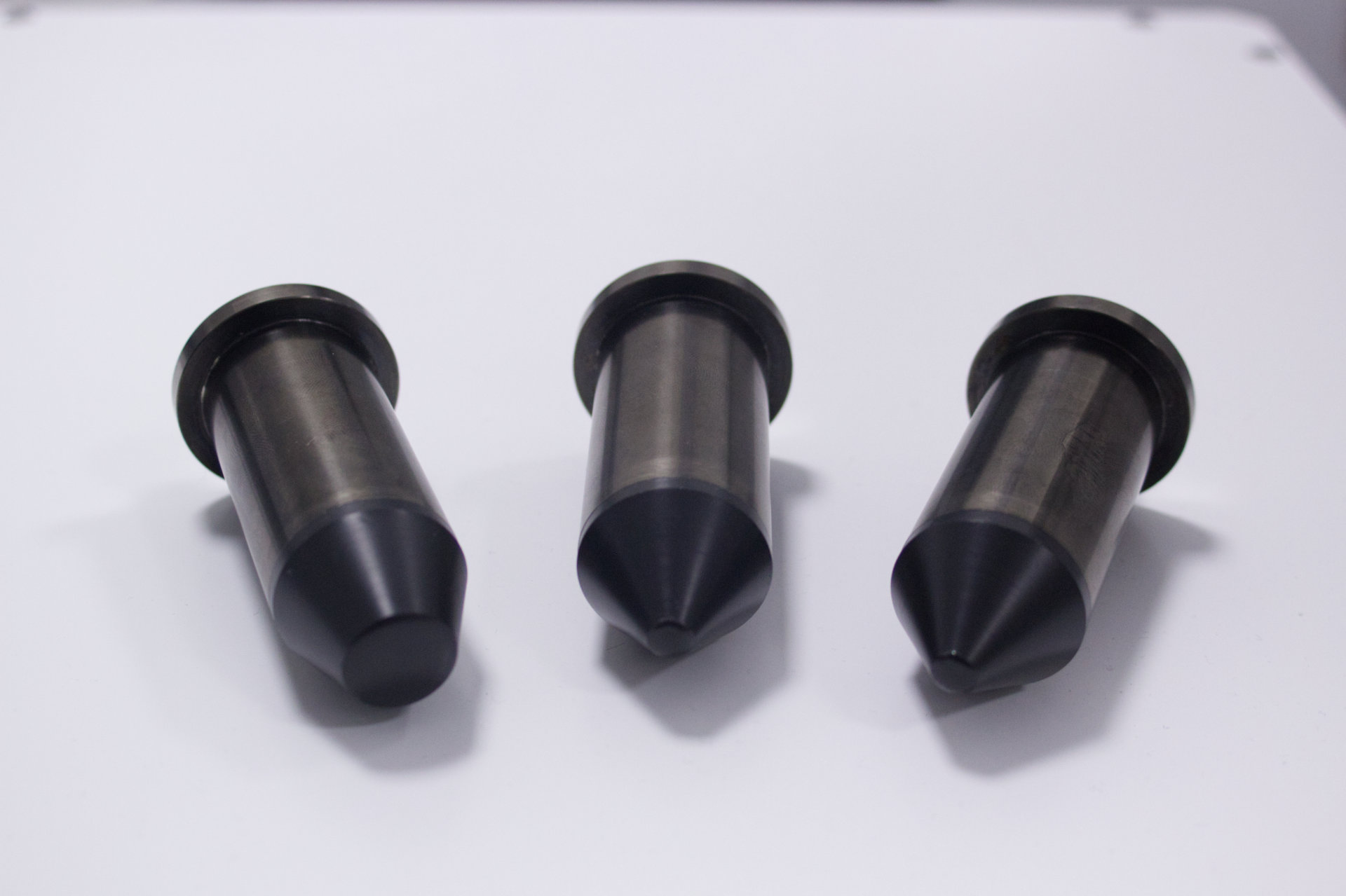
- Various sensor options to adjust the device optimal to your measurement task
- Tension Frame allowes to adapt the sensor z-position to follow the contour of the samples surface
Introduction
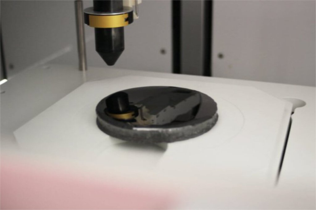
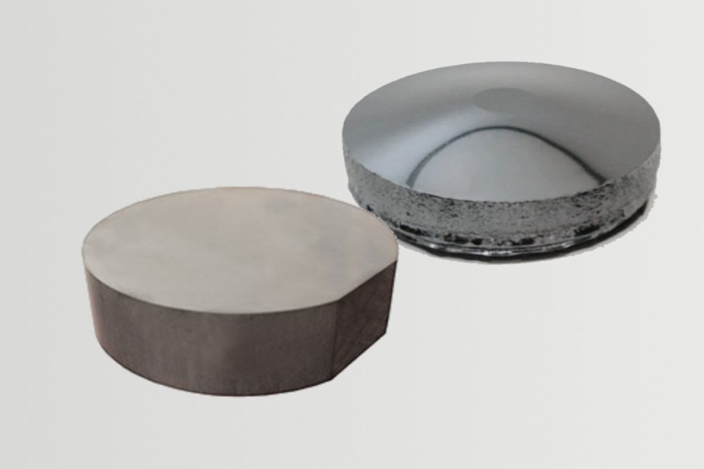
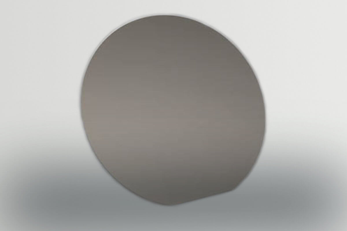
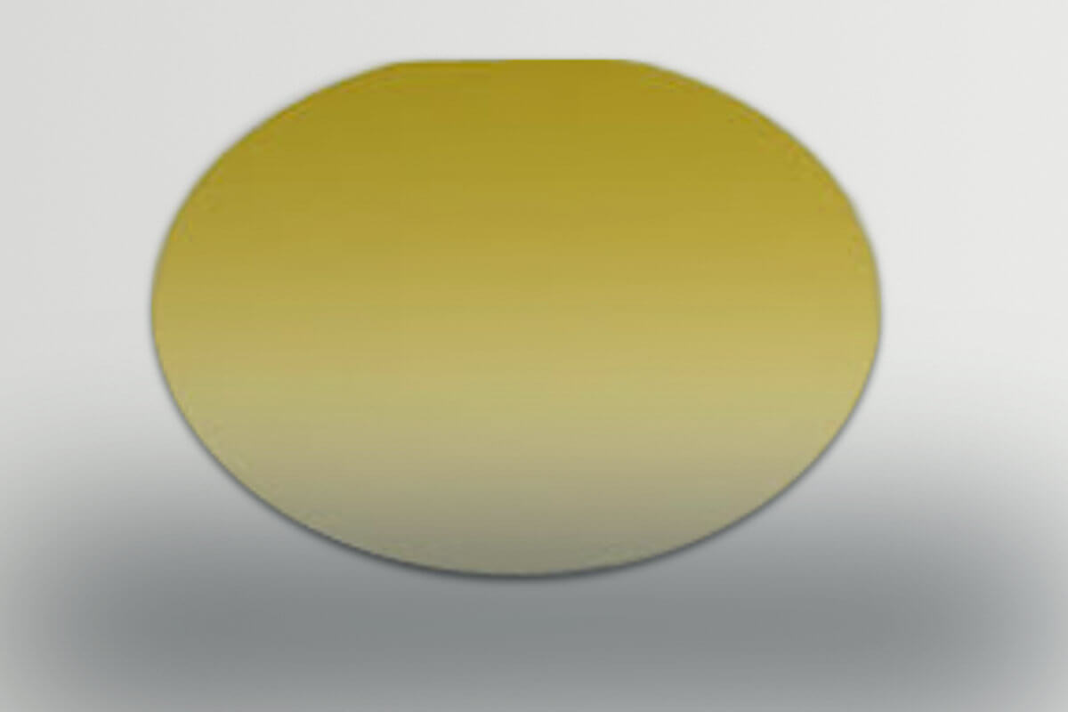
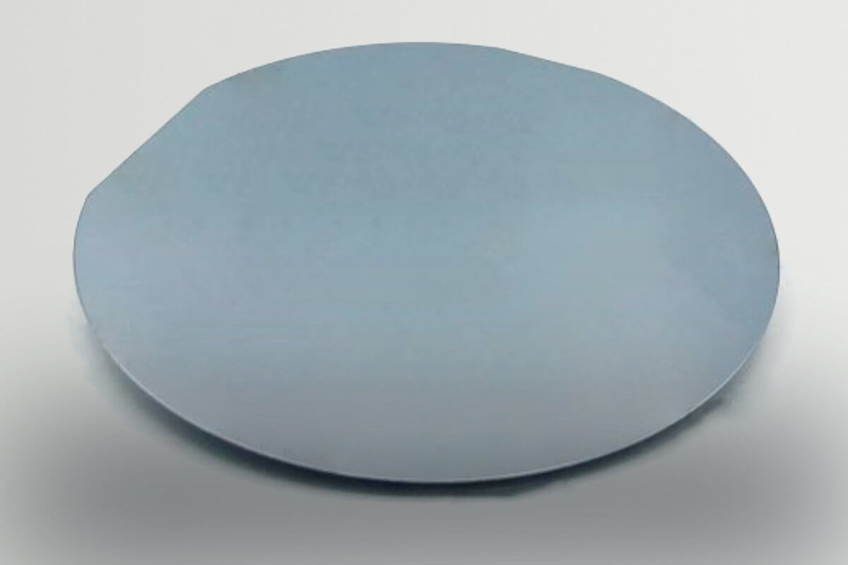
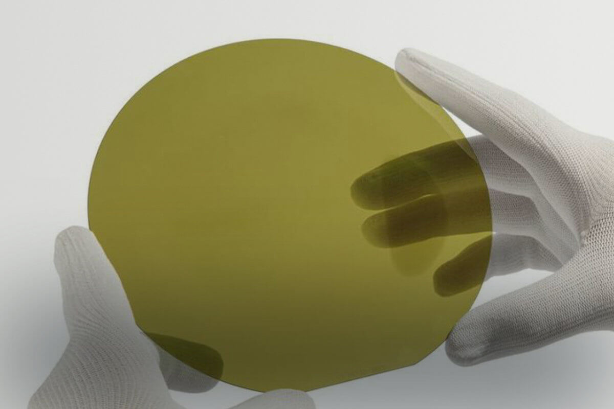
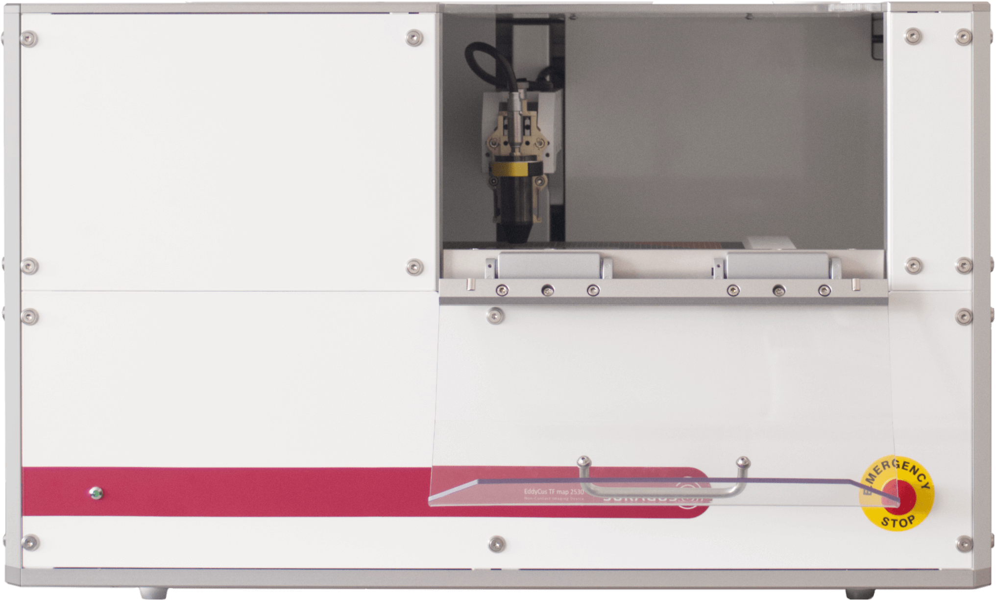
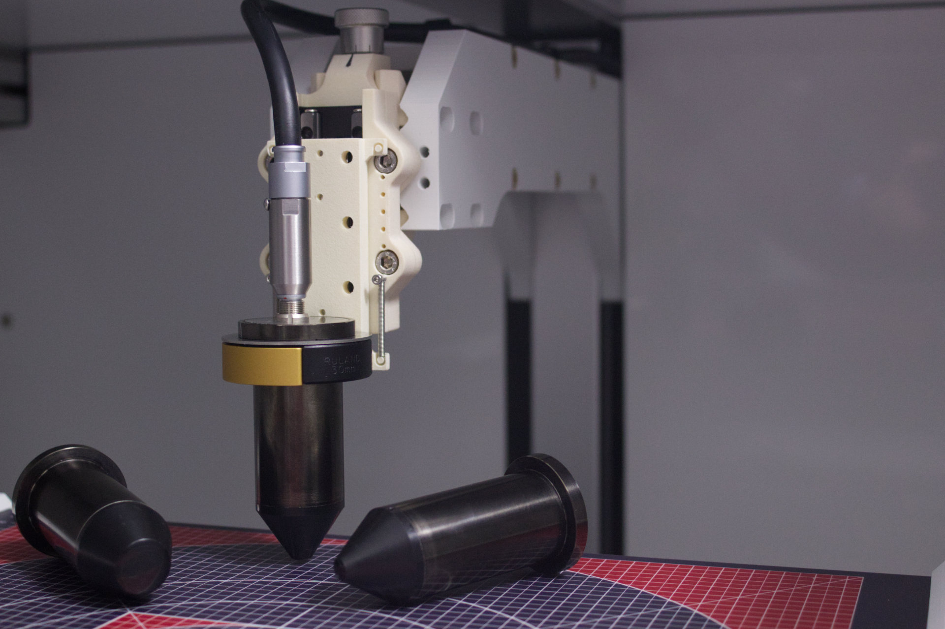
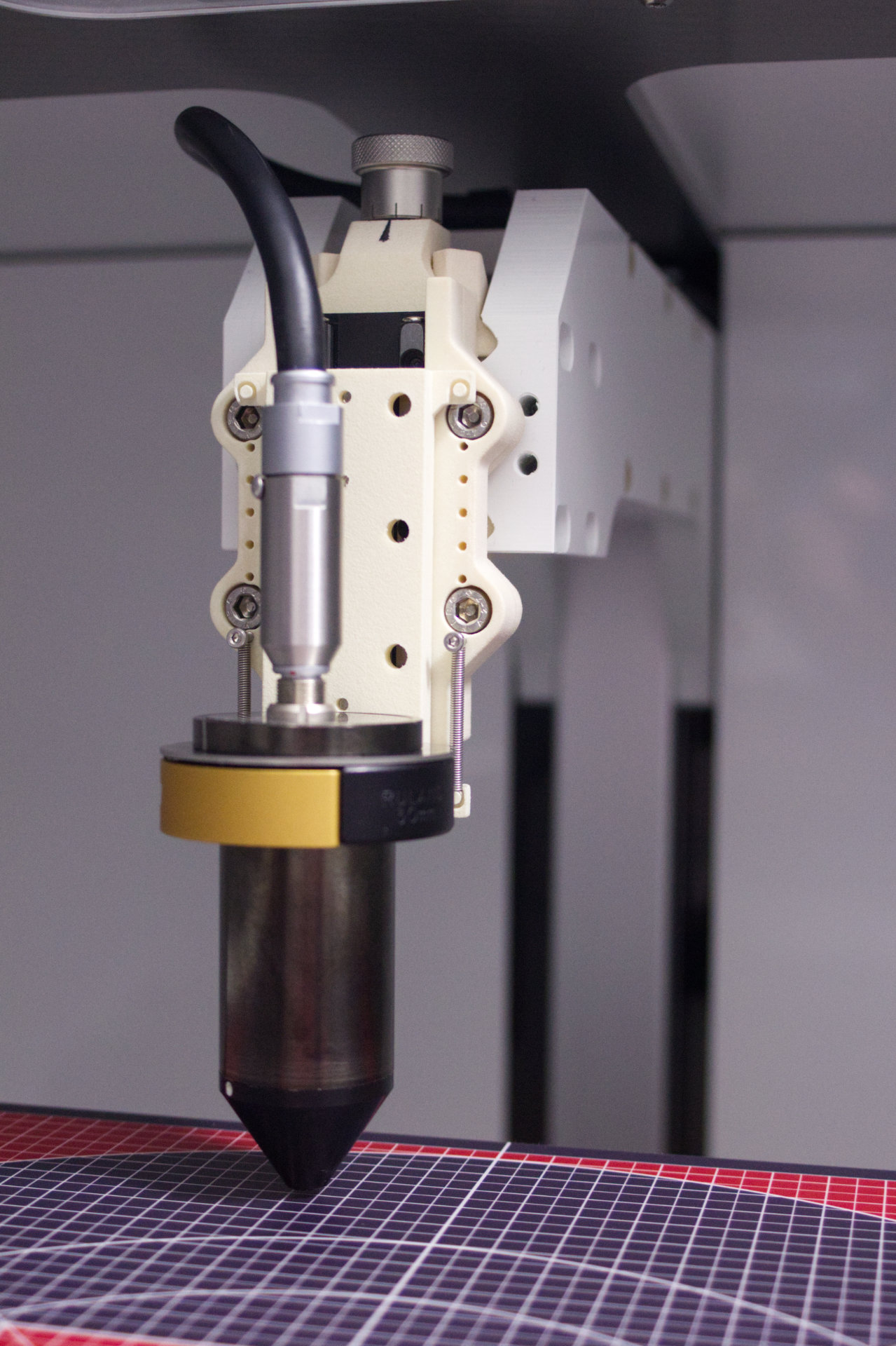
The EddyCus® map 2530 RMT is a bench top scanner particularly suitable for research and technology labs. It is fully functional to measure especially high samples with non-flat surfaces like boules but also for pucks and wafers. It’s a compact device, which can measure samples up to 300 mm (12 inch).
The device is typically used for:
- Shapes: bulk materials with curved surfaces
- Exchangeable sensors dedicated to specific measurement task
- Customized specimen holder in terms of layout and shape in favor to specimen dimensions
- Data analysis, export and reporting functions
- Measurement up to the edge
- Over 30 000 real measurement points for small defect detection
Sensor Capabilities
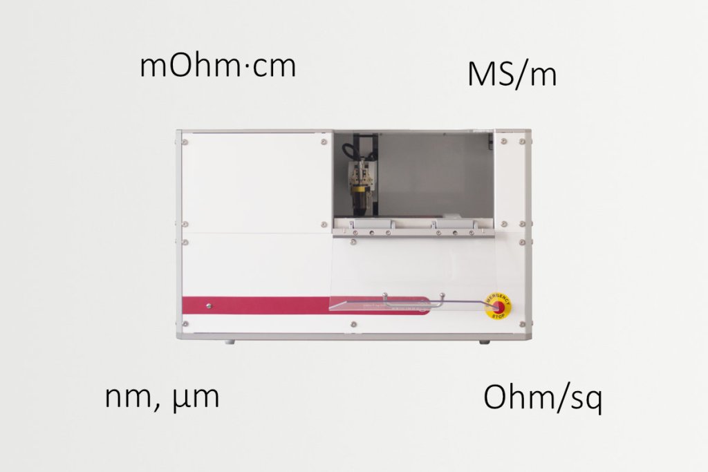
- Resistivity [0.1 – 100 mOhm·cm]
- Conductivity [0.01 – 65 MS/m]
- Sheet Resistance [depending on the resistivity]
- Metal Layer Thickness [2 nm – 2 mm]
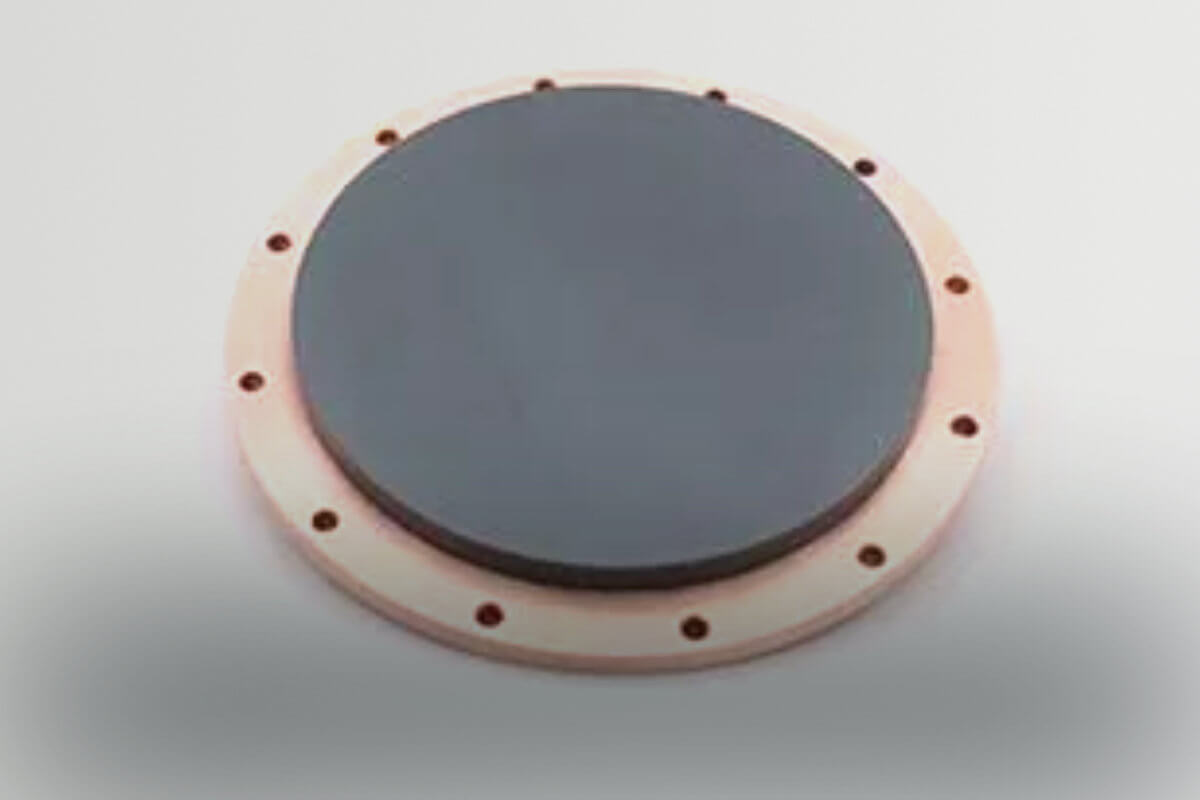
Supported Substrates
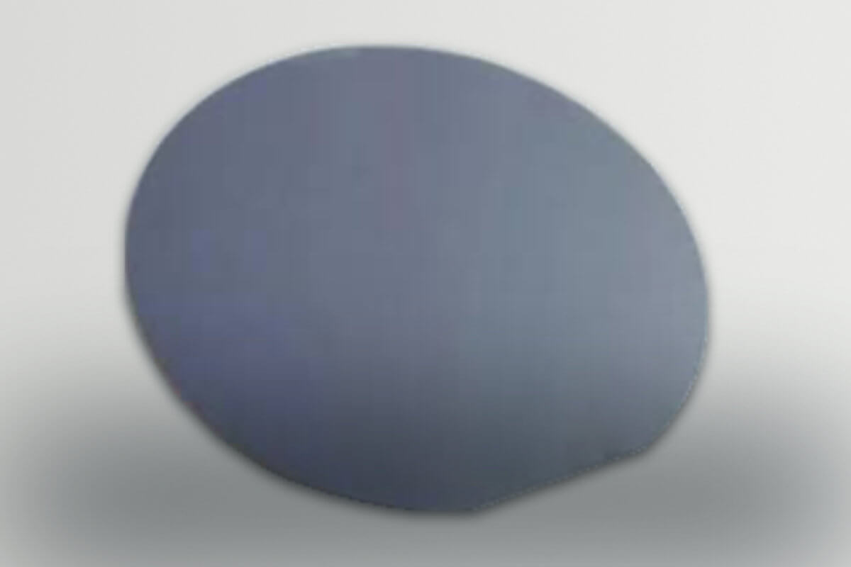
Boules, pucks and wafer
- Maximum height: 100 mm
- Maximum weight: 10 kg
Measurement Field
Sample sizes between Ø 150 mm and Ø 200 mm
Individual sizes upon request
Features and Benefits
2 – 12 Inch
High Sample Measurable
Various Analyzing Options
Measuring up to the Edge
Fast Results
High Resolution Mappings
Easy to Use
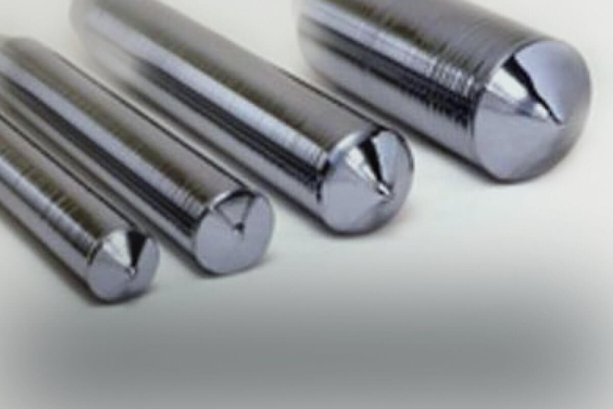
Curved Surfaces
Measuring up to the Edge
Due to the small spot size of up to only 1 mm of the SURAGUS Sensor XS the EddyCus® map 2530 RMT has a extreme good spatial resolution. Because of that the sensor can measure up to the edge of the sample. That helps to record true measurement values instead of using an extrapolating algorythm to generate an complete image of the sample.
High Resolution Mappings
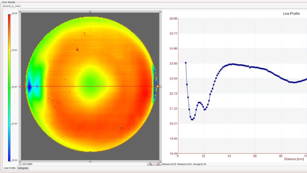
The resolution of a scan depends on the measurement pitch choosen in the recipe and the size of the sample. A boule, puck or wafer with a diameter of 300 mm can have between over 30,000 measurement points (1 mm pitch) to around 300 measurement points (10 mm pitch). The difference in scanning speed is factor 10. The sweet spot between a high resolution and a high speed is the 2.5 mm pitch. Scans with 2.5 mm pitch have around 5,000 real measurement points on a 300 mm boule, puck or wafer.
Due to the high resolution all information remain intact. No interpolation between the measurement points will generate additional information. Therefore a high resolution is crucial for the detection of small defects or imperfections.
To ensure the best possible scanning results, we offer a broad range of sensor types, each with its own strengths and limitations. We carefully analyze each measurement task to determine which sensor is best suited, guaranteeing optimal performance for your specific needs.
One Device, Multiple Measurement Parameters
The EddyCus® map 2530 RMT is able to measure different measurement parameters. The resistivity correlates with sheet resistance and metal layer thickness. As long as the material is well known all of these measurement parameters can be measured precisely.
- Resistivity
- Conductivity
- Sheet resistance
- Metal layer thickness
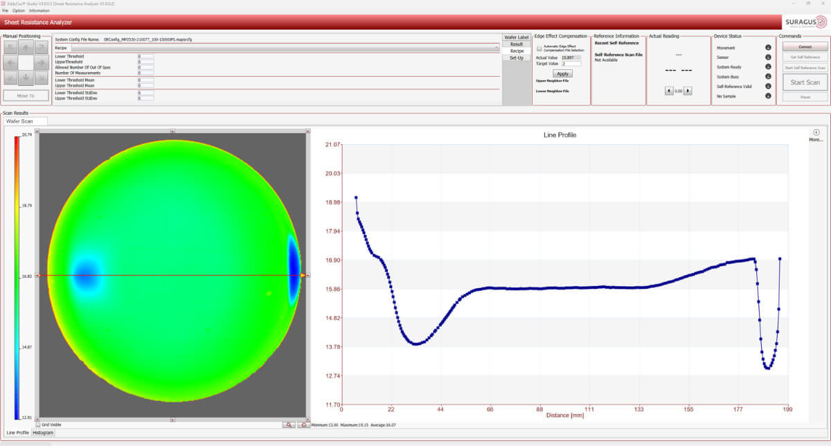
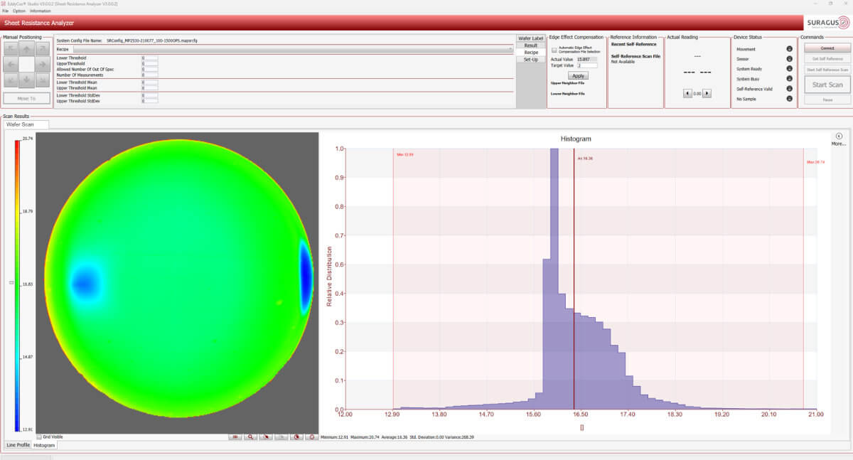
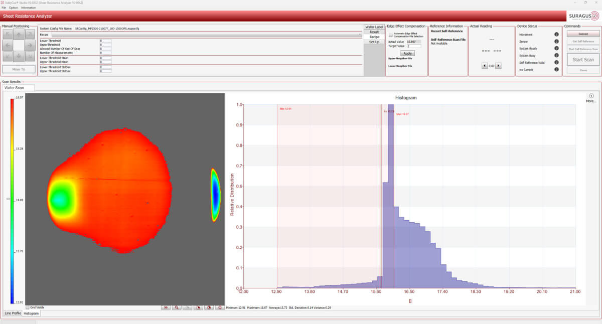
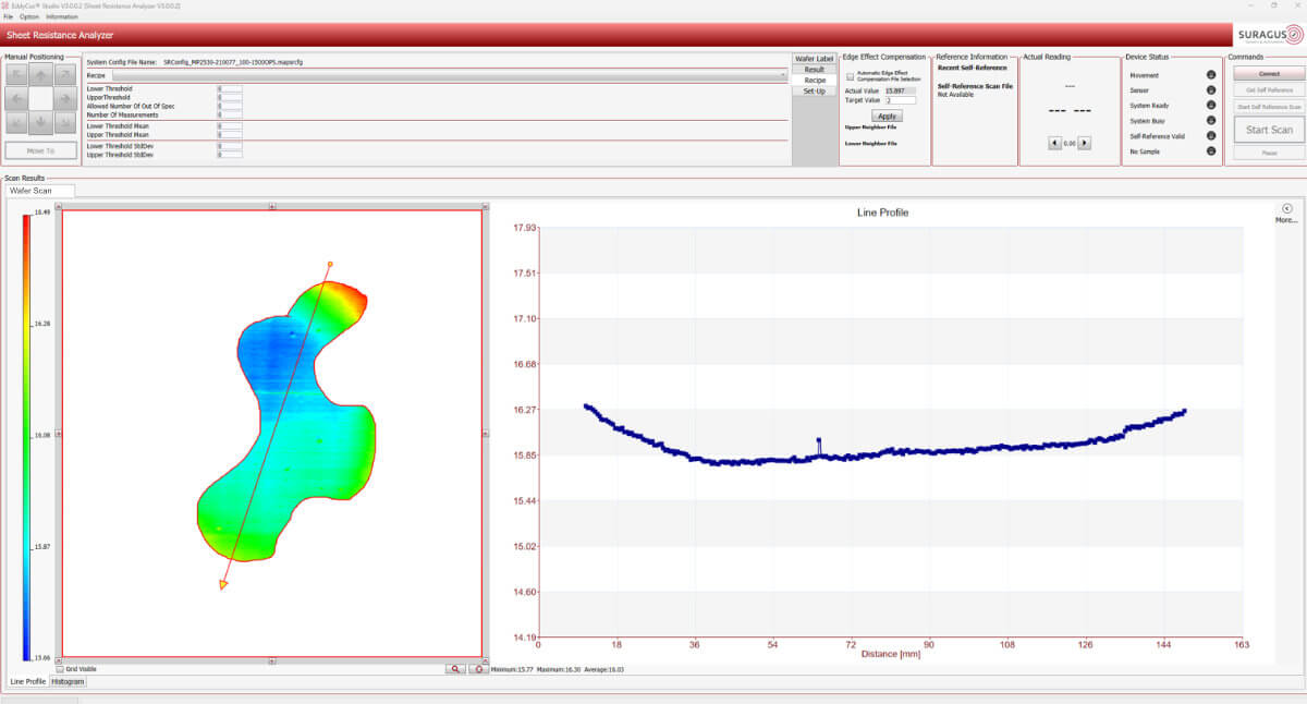
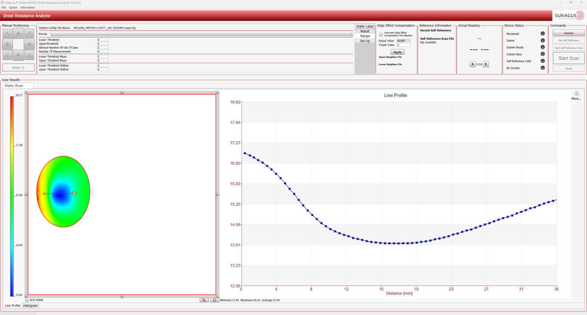
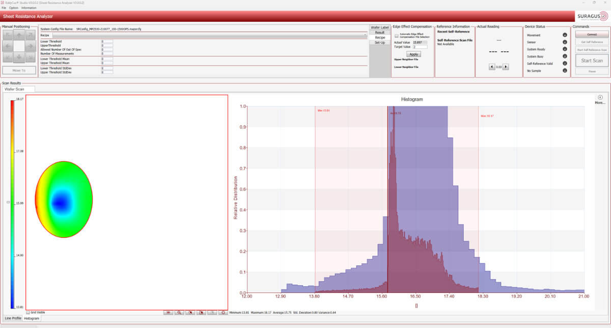
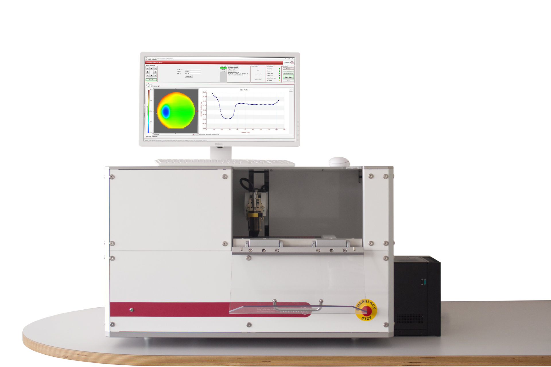
Easy to Use Software With Various Analyzing Options
The EddyCus® map 2530 RMT for boules, pucks and wafers has an easy to use software. After you laid your sample central on the measurement field you
Choose your recipe
Press on “Start”
Watch the software creating the map while scan process proceeds
After the scan is finished you can start the analyzing process. You will be able to
- Draw line profiles
- Predefined line profiles and
- Free drawed line profiles
- Draw specific areas of interest
- Rectangle
- Circle
- Pen to draw free area
- Select a histogram
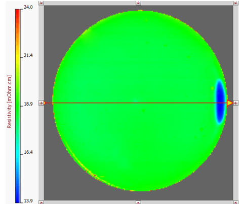
Sheet Resistance Imaging
Metal Layer Thickness Imaging
Resistivity Imaging
Electrical Anisotropy Imaging
Video of the EddyCus® map 2530 RMT
The video gives you an impression of how to use the map 2530 RMT. Which materials can be analysed and how the device works in general.
For Various Sizes of Boules, Pucks and Wafers
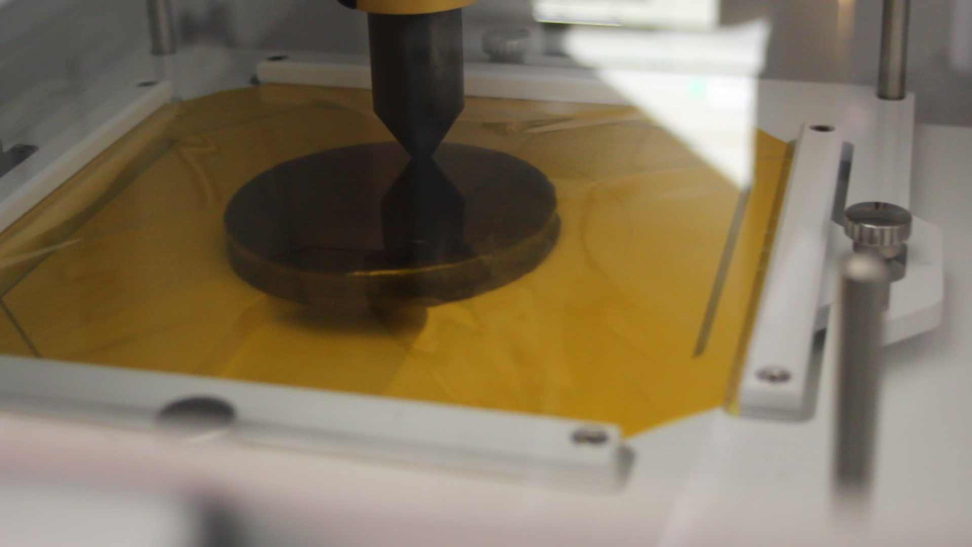
For optimal results, it is crucial to position the samples precisely at the center. The inlays are available for samples of various diameters, up to 205 mm. They simplify and accelerate the positioning process, eliminating a potential source of error and ensuring more reliable results.
Curved and High Samples like Boules and Pucks
The puck and boule imaging device can measure samples with heights of up to 100 mm and a maximum boule curvature of 10 mm. It can also scan thin samples such as wafers. The device supports sample weights of up to 10 kg, which corresponds to a SiC puck measuring 300 mm in diameter and 100 mm in height. If you need to measure heavier samples, please contact us for more information.
Data Table for EddyCus® map 2530 RMT
Device Features
| Measurement technology | High frequency eddy current sensor |
| Substrates | Boules, pucks, wafers |
| Substrate area | 12 inch / 305 mm x 305 mm (larger upon request) |
| Edge effect correction / exclusion | 2 – 10 mm (depending on size, range, setup and requirements) |
| Max. sample thickness / sensor gap | 100 mm |
| Max. sample weight | 10 kg |
| Scanning pitch | 0.1 / 1 / 2.5 / 5 / 10 mm (other upon request) |
| Spot size (coil size) Penetration depth (frequency) |
1 – 9 mm (depending on coil size) 1 – 10 mm (depending on frequency) |
| Measurement points per time (square shaped samples) | 100 measurement points in 0.5 minutes 10,000 measurement points in 3 minutes |
| Speed | 150 mm per second (time 1 to 30 minutes) |
| Available measurement features | Sheet resistance map Conductivity map Resistivity map Electrical anisotropy map Permeability map (beta) |
| Device dimensions (w/h/d) | 31.5” x 19.1” x 33.5” / 785 mm x 486 mm x 850 mm |
| Weight | 90 kg |
Measurement Capabilities
| Resistivity measurement | |
|---|---|
| Resistivity measurement range |
0.1 – 1 mOhm·cm; 2 – 5 % accuracy 1 – 10 mOhm·cm; 1 – 3 % accuracy 10 – 30 mOhm·cm; 1 – 3 % accuracy 30 – 100 mOhm·cm; 1 – 3 % accuracy |
Conductivity measurement |
| Conductivity measurement range | 0.01 – 65 MS/m | Sheet resistance measurement |
| Sheet resistance measurement range |
0.05 – 0.1 mOhm/sq; 1 – 2 % accuracy 0.1 – 10 mOhm/sq; 1 – 2 % accuracy 10 – 100 mOhm/sq; 1 – 2 % accuracy 100 – 1,000 mOhm/sq; 1 – 2 % accuracy 1,000 – 10,000 mOhm/sq; 1 – 2 % accuracy |
Metal layer thickness measurement |
|
Metal layer thickness measurement range |
Metal thickness measurement by conversion or direct calibration |
Frequently Asked Questions
Sheet resistance, metal layer thickness, resistivity, conductivity
Sizes up to 300 mm (others on request)