Thin film PV module manufacturer have to adress highest quality in contact and absorber layer deposition. These processes are mainly driven by physical vapour deposition (PVD) and heating cycles close to glass softening point. To ensure highest efficiency in solar module at lowest manufacturing cost following processes have to be monitored:
Back contact
Front contact
Electrodes
Buffer or seed layer
Testing
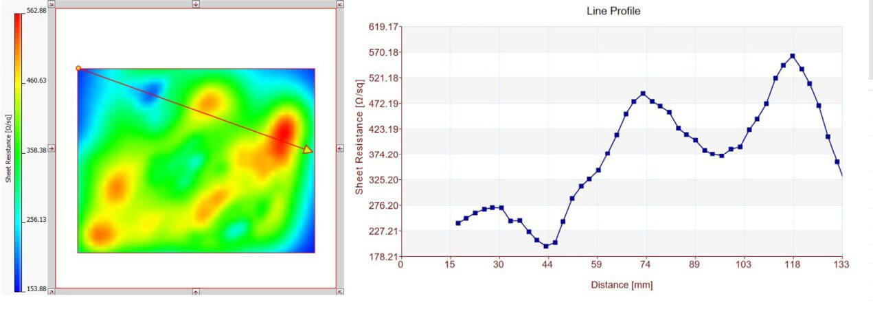
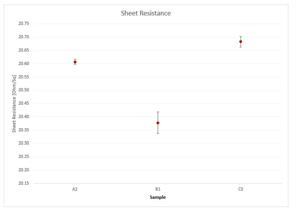
Sheet resistance
Conductivity
Thickness
Homogeneity
Permeability
Applications
Deposition process control
Heating process control
Quality control
Final inspection
Substrates
Glass
Plastic film
Process
S2S
R2R
Environment
In-vacuo and ex-vacuo
In-situ and ex-situ
Inline and offline
Types
CdTe
CIGS
Perovskite
Organic (OPV)
Tandem
Use Case Back Contact
Organic PV cell manufacutring reqiures smooth back contact electrodes. Eddy Current Technologiy enables monitoring and quality assurence of AgNW deposition processes.
Use Case Cell or Module Integrated TCO Front Contact
Characterizing cell integrated front contacts in a superstarte configuratioin is challenging. Eddy current technologiy utilizes anisotropic properties to separate the electromagnetic field of the front contact from the electromagnetic field of the back contact. Hence, sheet resistance of cell integrated front contact of a manufacutred thin film PV mdoule can be characterized.