
Wafer Metallization Characterization
Characterize aluminum metallization uniformity and sheet resistance on wafer level to optimize device performance
- Non-contact and non-destructive
- Near-process monitoring
- High Resolution Imaging
- High-speed and accurate
- High repeatability and long term stability
- Test directly on product wafers
- Easy integration into tools
Challenges for Wafer Metallization Product Quality
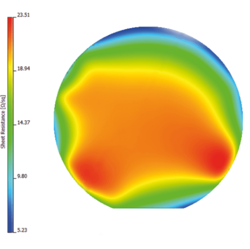
Aluminum interconnects on silicon wafers typically show sheet resistance from 0.03 to 0.13 Ohm/sq at film thickness between 0.2 and 1 micrometer. Keeping layer thickness and uniformity within tight limits is challenging, since even small drifts directly impact product quality, compliance with minimum specifications and material consumption. At the same time, stable sheet resistance and high lateral homogeneity are required to avoid local hot spots, timing shifts and early reliability failures. Defects such as voids, hillocks or particles can turn marginal areas into open or leaky lines, which makes detailed wafer level mapping of thickness, sheet resistance and defect distribution essential for robust interconnect processes.
Atline Analysis Solution for Metallization Characterization on Wafer
EddyCus® map 2530 TM imaging devices specialized for metallization layers or the fully automated EddyCus® ResMapper
With a sheet resistance range from 0.001 to 20,000 Ohm/sq, the EddyCus® map 2530 series is ideal for the characterization of aluminum metallization on wafers.
It is also suitable for other metallizations such as
- Copper – Cu
- Titatnium nitride – TiN
- Tantalum nitride – TaN
- Nickel – Ni
- ITO
Inline Analysis Solution for Wafer Metallization Characterization
The EddyCus® inline SLIM is part of our family of in tool metrology solutions. These systems are integrated directly into vacuum deposition chambers and generate line profiles of sheet resistance, layer thickness and resistivity immediately after coating. This provides instant feedback on process stability and product quality.
The data quality is comparable to that of conventional four point probe systems.
Measurement Results
Installing the EddyCus inline SLIM is quick and non invasive. The existing valve lid is replaced by a lid with an opening for the cable feedthrough. The deposition tool remains in place and keeps its qualification.
Simple retrofit workflow
- Remove the original cover
- Remove the valve
- Insert the sensor fork into the wafer transfer path
- Mount the valve again
- Route the cable through the prepared opening
- Install the replacement cover with cable feedthrough to the control unit
- System is ready for measurement
Typical installation time is within one hour.
Conclusion
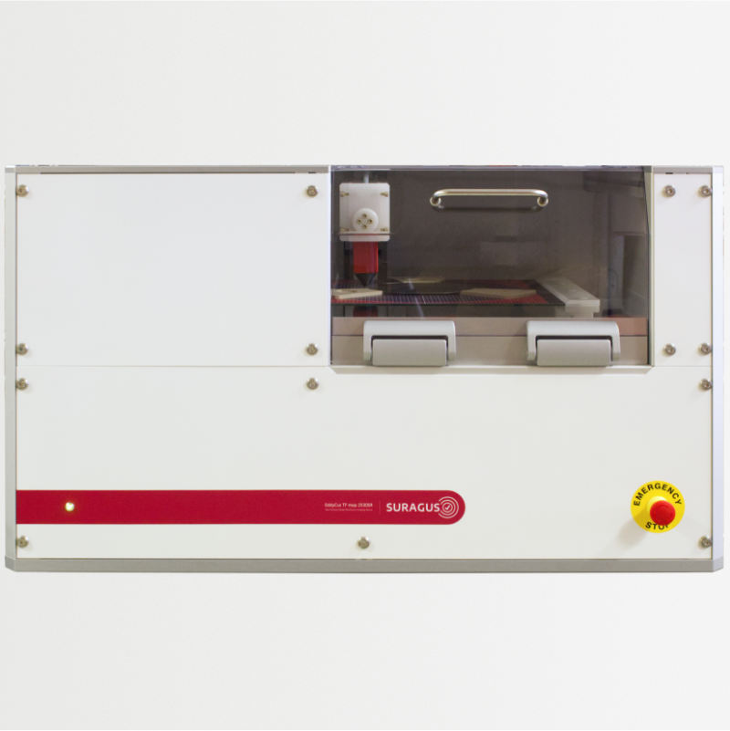
Semi-automated
EddyCus® map 2530 Series
Eddy current in-tool measurement transforms vacuum deposition from a periodic, test-wafer-driven process into a continuous, data-driven, self-monitoring system. By providing real-time thickness feedback on actual production wafers, it:
- Shortens qualification cycles
- Reduces measurement latency
- Minimizes uncertainty
- Cuts the need for dedicated monitor and test wafers
As a result, fabs achieve higher throughput, lower cost of ownership, and significantly reduced non-productive wafer usage, while maintaining or even improving process stability and uniformity.
Eddy current and four point probe measurements correlate closely.
Click here to see a detailed comparison.
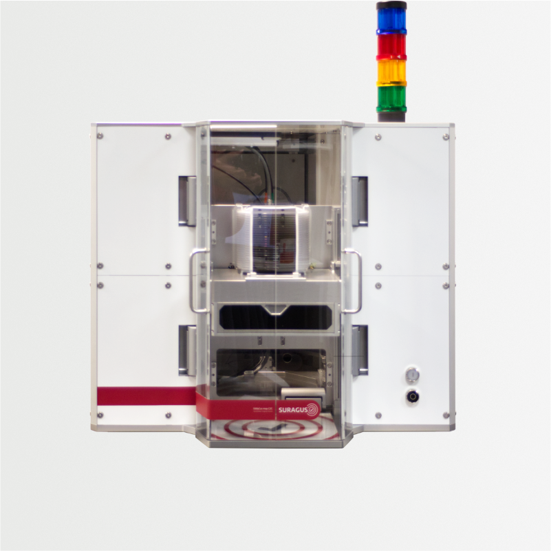
Fully-automated
EddyCus® ResMapper
Eddy current in-tool measurement transforms vacuum deposition from a periodic, test-wafer-driven process into a continuous, data-driven, self-monitoring system. By providing real-time thickness feedback on actual production wafers, it:
- Shortens qualification cycles
- Reduces measurement latency
- Minimizes uncertainty
- Cuts the need for dedicated monitor and test wafers
As a result, fabs achieve higher throughput, lower cost of ownership, and significantly reduced non-productive wafer usage, while maintaining or even improving process stability and uniformity.
Eddy current and four point probe measurements correlate closely.
Click here to see a detailed comparison.
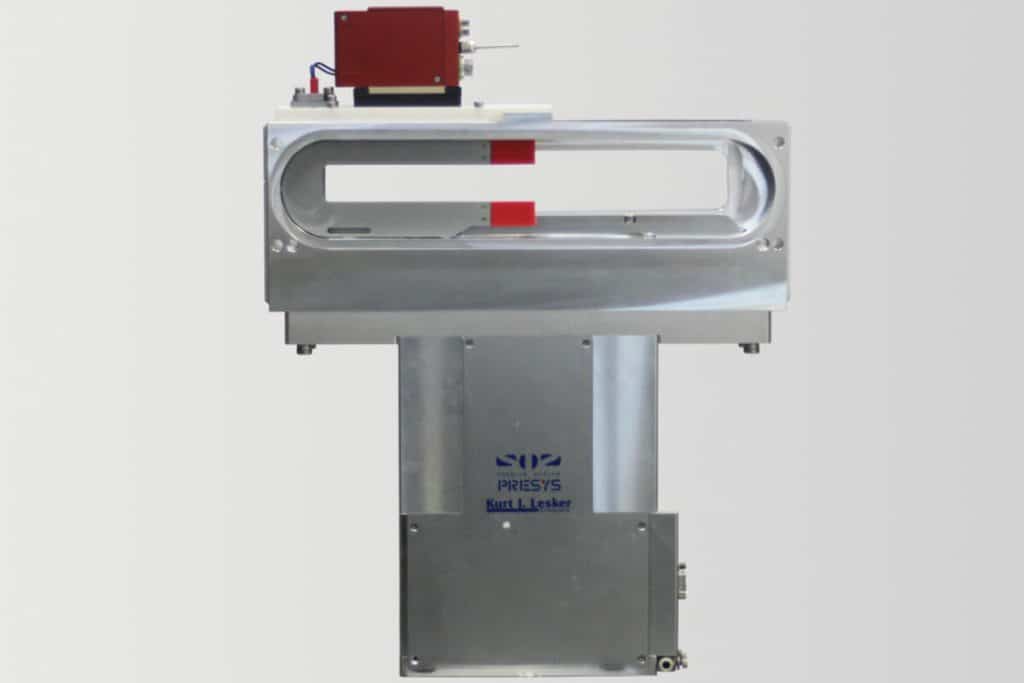
In-chamber inline
EddyCus® inline SLIM
Eddy current in-tool measurement transforms vacuum deposition from a periodic, test-wafer-driven process into a continuous, data-driven, self-monitoring system. By providing real-time thickness feedback on actual production wafers, it:
- Shortens qualification cycles
- Reduces measurement latency
- Minimizes uncertainty
- Cuts the need for dedicated monitor and test wafers
As a result, fabs achieve higher throughput, lower cost of ownership, and significantly reduced non-productive wafer usage, while maintaining or even improving process stability and uniformity.
Eddy current and four point probe measurements correlate closely.
Click here to see a detailed comparison.
Request a Quote
You can use the formular to write us a message.
Frequently Asked Questions
- Sheet resistance
- Metal layer thickness
- Resistivity
- 150 mm,
- 200 mm and
- 300 mm samples
- 2 – 4 inch wafers via adapters
- Sheet resistance line profile
- Metal layer thickness line profile
- Resistivity line profile