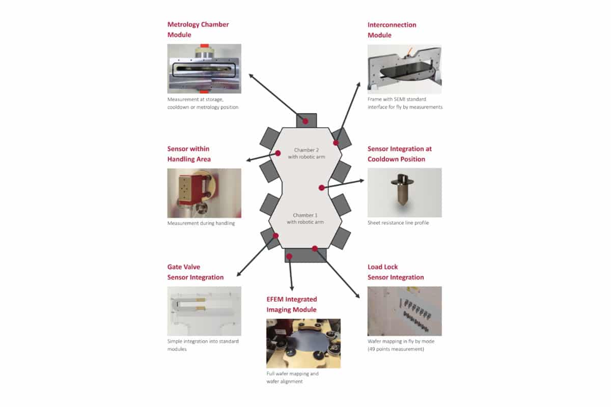
Sensor integration kit for automated wafer handling platform based on non-contact eddy current sensors
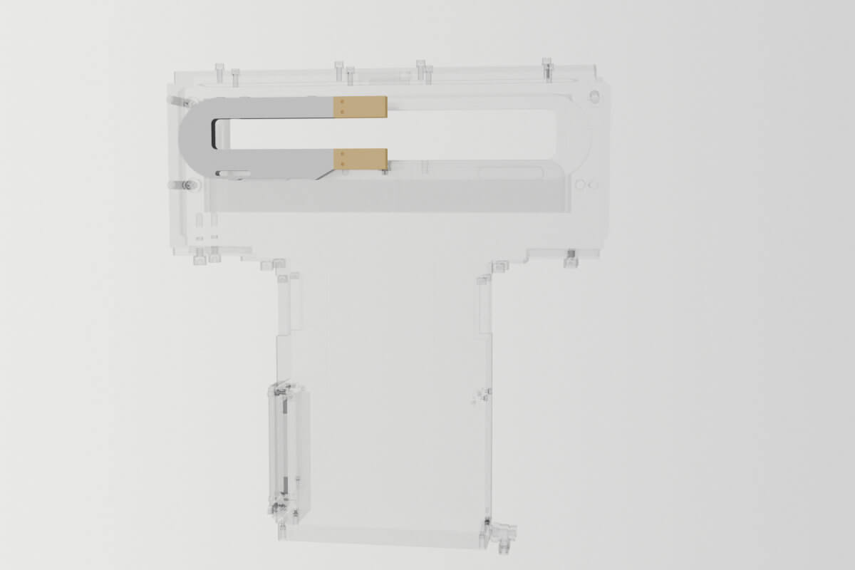
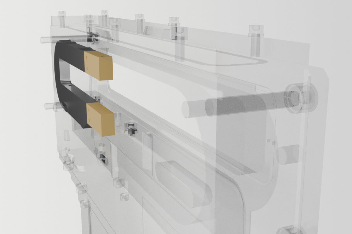
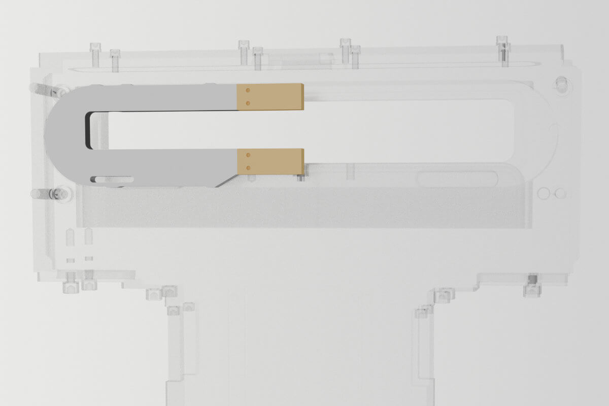
Gate Valve and Transfer Sensor Integration Kit
Gate valve between the handling chamber and the deposition chamber, can be equipped with an integrated non-contact eddy current sensor for line profile measurement
Distance between the sensor and the substrat is at least 20 mm
Challenges Today
Vacuum and wet process fabs consume large volumes of test afers every month to verify sheet resistance and metal layer thickness, with each qualification cycle pulling 3 to 5 dedicated wafers through 5 to 7 reclaim steps and waiting 1 to 48 hours for offline four-point-probe results. This procedure has several implications, discussed in this edition.
Process Monitoring across:
PVD
ALD
CVD
Etch/RIE
CMP
Conductive films, barriers, liners, power metal
3 Structural Challenges
3 Structural Challenges
Hours of Delay
Offline 4PP feedback arrives 1-48 h later. The tool waits idle or runs blind on real product.
Wasted Expense
Test wafer, storage, transportation, handling, floor space and 5-7 reclaim steps per cycle. 30-50 % of test wafers (careful industry estimate) exist solely for Rs verification, burning capital that never touches a product wafer.
Product Wafers Never Measured
Drift, edge uniformity and real film properties stay invisible. Test wafers differ from product in stress, nucleation and oxidation.
4PP and Eddy Current measurement have been standard for decades before appearing as SEMI standard in 2002. SURAGUS advancements in signal processing allow the measurement in wafer fly-by mode. The history is here:
1969
SEMI MF84
4PP base standard
1988
SEMI MF673
Eddy Current Rs
1990
SEMI MF374
4PP epitaxial layers
2000
SEMI MF1529
4PP automated wafer mapping
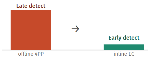
Using 4PP instead of Eddy Current is like using an analogue camera in the digital era.
For decades, sheet-resistance verification has meant the same workflow: pull a dedicated test wafer, push it to an offline four-point probe, and wait hours for an answer that arrives long after the product has moved on. In-tool eddy current measurement changes the location and the timing. The wafer being measured is the product wafer itself, inside the process tool, in vacuum, with the result available the moment the wafer moves.
It is the same shift the imaging world made a generation ago. With analog film, you framed the shot and waited days for the lab to develop it; with digital photography, the result appears the instant the shutter closes. The development time of your data has changed dramatically.
Seven Value Drivers – At a Glance
The first wafer in spec is the last test wafer. The next wafer can be product.
Scrap / Rework Cascade
H1
Drift visible from wafer #1 – not hours later
Lot-scale exposure shrinks to single-wafer exposure
Avoids whole-lot scrap events
Realtime Qualification
H2
Tool qualification time: few seconds only with EC
Tool usage is revenue-oriented, no idle period
Regain Lost Capacity
Priority Lot Confidence
H3
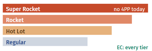
Demonstrator lots fly blind today – EC gives data without stopping
All hot lots verified in real time, every priority tier covered
Complete Control and Confidence
NPW Reduction
H4
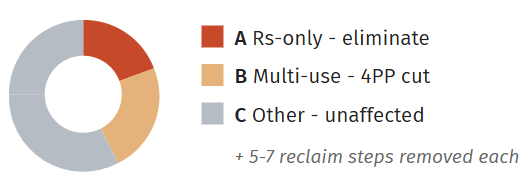
Category A wafers fully eliminated
Category B retains the wafer, removes the 4PP step
Reduce Unnecessary Costs
Sheet Resistance Range Upgrade
H5
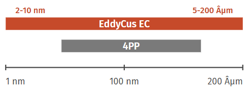
Thin barriers (TaN, TiN at 2-10 nm) – 4PP unreliable
Thick power metal (5-200 µm Cu/Al) – below 4PP sensitivity
Where 4PP fails, EC delivers
Edge Characterization
H6
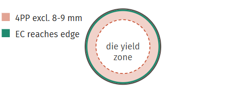
4PP edge exclusion: 5-6 mm from film, 8-9 mm from wafer edge
EC: algorithmic correction to the film edge itself
More Sellable Die
Real Product Wafer, Real Process Conditions
H7
A product wafer is not a test wafer. It carries different thermal mass, different warpage when processed hot, different surface chemistry, and different stress history. EC measures the real wafer, in vacuum, under genuine process conditions, before oxidation.
In-tool eddy current measurement creates value across seven distinct operational and technical dimensions. Each one stands alone; together they reshape the economics of vacuum deposition. Figures below are illustrative of typical multi-tool fabs and should be validated against each customer’s own data.