Contact Us
Do you need help with product selection?
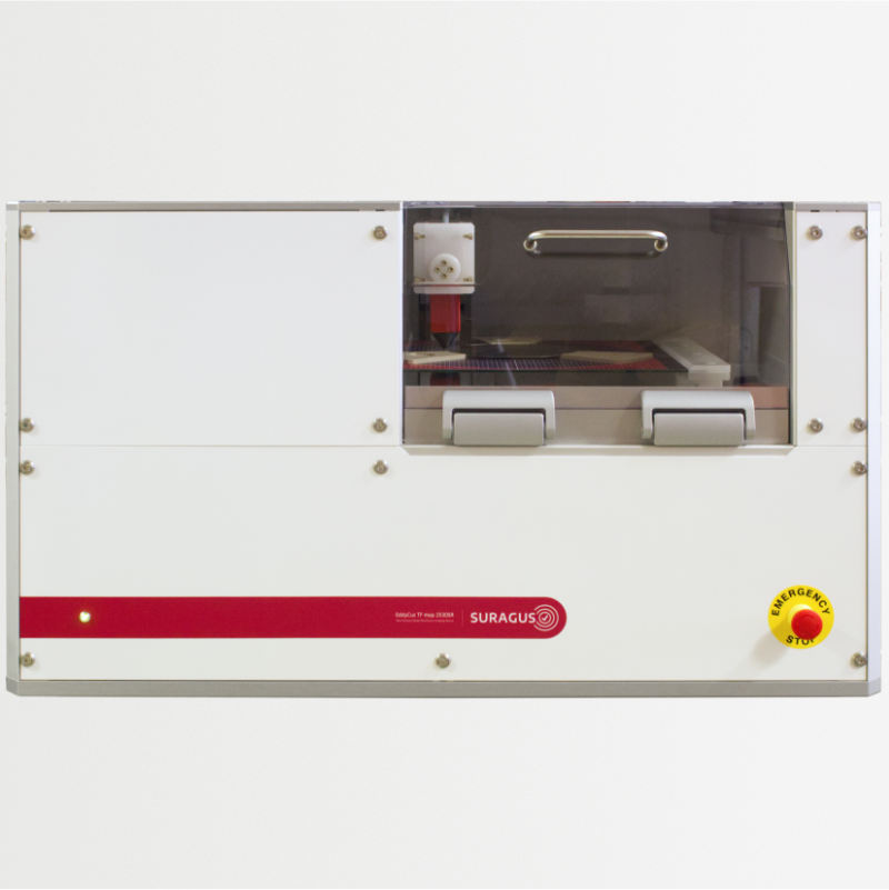
EddyCus® map 2530 RMT – Mixed Solutions
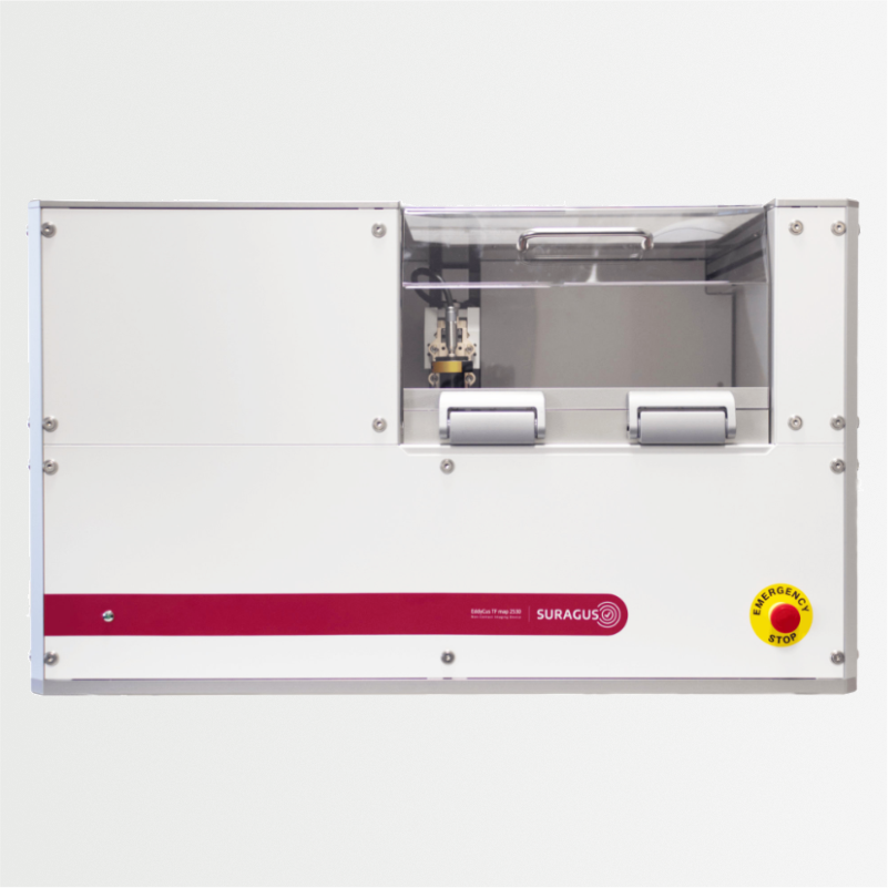
Multi Application Imaging Device Higher Thin-film and substrate quality through fast and precise mapping devices based on non-contact eddy current technology. High resolution images with over 30 000 measurement points within 4 minutes for best defect detection Measurement up to the edge of the sample Various analyzing options such as line profiles or histogram Various […]
EddyCus® map 2530 RMT
Resistvity Mapping and Defect Identification for Boules and Pucks Fast, precise mapping with non-contact eddy current technology improves thin-film and substrate quality. The short distance to the sample boosts signal strength and allows for a smaller spot size, enabling measurements close to the edge. High resolution images with over 30 000 measurement points within 4 […]
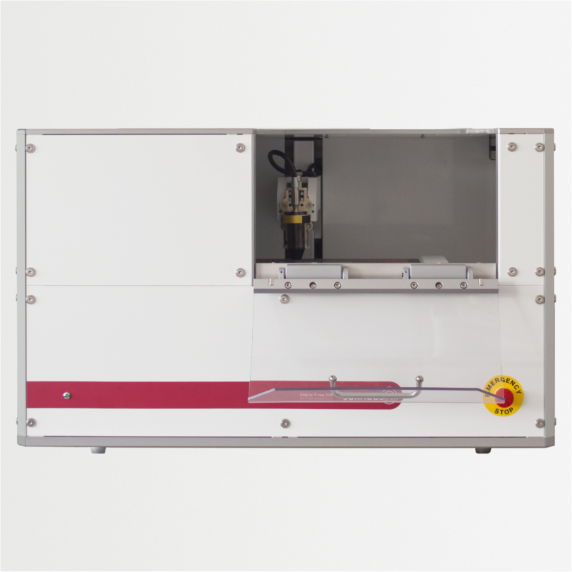
EddyCus® map 2530 RMB for Wafer and Metallizations
Mapping of Wafers and Metallization Layers Improved thin-film and substrate quality is achieved through high-resolution mapping enabled by non-contact eddy current technology. The EddyCus® map 2530 RMB, with its minimal spot size, allows for precise measurements in close proximity to the sample edge. Non-contact Fast and precise measurement High resolution mapping of conductive thin films […]
EddyCus® map 2530 RMB
Resistvity Mapping and Defect Identification for Boules, Pucks, Ingots and Wafers Enhanced thin-film and substrate quality through fast, precise mapping using non-contact eddy current technology. Designed for bulk materials like SiC or Si pucks up to 5 kg and 200 mm in height, with additional capability to measure wafers. Non-contact Fast and precise measurement High resolution mapping […]
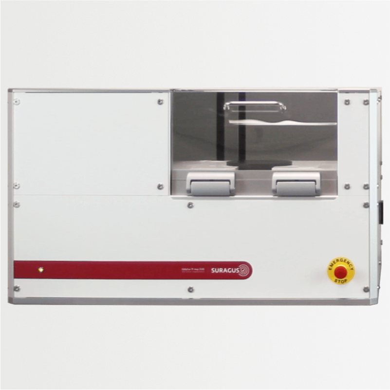
EddyCus® map 2530 TM
Non-contact Sheet Resistance and Metal Layer Thickness Mapping Device Improve thin-film and substrate quality with fast, precise, non-contact mapping. The device accurately measures sheet resistance and correlating parameters in wafers, foils, glass, and metallized layers. Non-contact Fast and precise measurement High resolution mapping of conductive thin films Imaging of substrates up to 300 x 300 […]