sp table test
sp table
SURAGUS Product Overview SURAGUS Product Overview Non-contact eddy current measurement systems for sheet resistance, layer thickness, resistivity, and further electrical parameters – from handheld devices to full inline integration. Single Point – Handheld & Benchtop ‹ › Handheld EddyCus® Portable Portable handheld device for non-contact sheet resistance measurement directly on-site. Instant results on the integrated […]
Parameter Matrix
Parameters We Measure Our precision instruments cover a comprehensive range of measurement parameters for industrial applications. Sheet Resistance 8 µΩ/sq – 300,000 Ω/sq Metal Layer Thickness 1 nm – 2 mm Resistivity 1 – 3,000 mΩ·cm Electrical Anisotropy 0.33 – 3 MD/TD Emissivity 0.003 – 0.5 Areal Weight 1 – 100 g/m² Defects & Geometry […]
Product Matrix
Overview of SURAGUS Products Single Point Measurement Solutions EddyCus® Portable Handheld for quick checks of flat materials EddyCus® Portable PS Handheld with external sensor for quick checks of bulk materials or curved surfaces EddyCus® lab 2020 TM Benchtop for flat materials such as foils, wafer or glass EddyCus® lab 2020 RMB Benchtop for bulk materials […]
Thickness Measurement for Feed Forward Etch Process Control
Inline Thickness Measurement for Feed-Forward Etch Process Control Enabling Sub-Nanometer CD Uniformity Through Pre-Etch Film Characterization As semiconductor devices continue to scale toward atomic dimensions, the margin for process variation has shrunk dramatically. At the 5 nm technology node, allowable critical dimension (CD) variation across the wafer is less than 0.5 nm—equivalent to just two […]
CMP Process Monitoring and Endpoint Detection
CMP Process Monitoring and Endpoint Detection Enabling Real Time Metal Film Thickness Measurement for Precision Planarization Control Chemical Mechanical Planarization (CMP) is an indispensable process in modern semiconductor manufacturing, enabling the global planarization required for multilevel interconnect structures at advanced technology nodes.As device geometries shrink below 10 nm and interconnect layers exceed 20 levels, precise […]
EddyCus® map IK
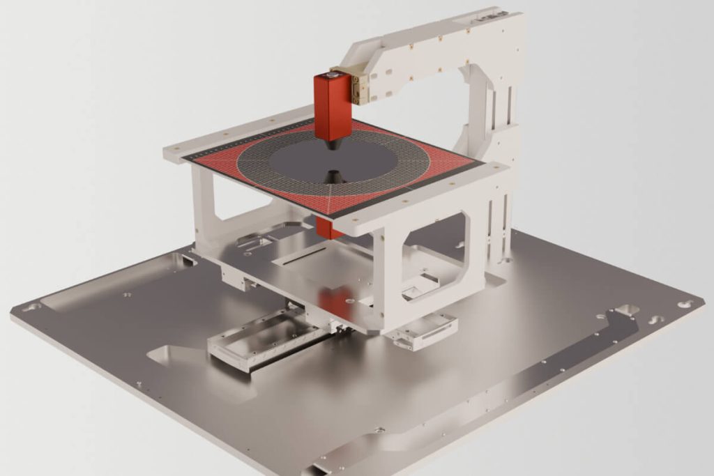
Non-contact Eddy Current Mapping Integration Kit for Sheet Resistance, Film Thickness and Resistivity Imaging Modular Sensor mapping integration kit to generate metal thinfilm thickness, sheet resistance or resistivity images of wafers, pucks and boules High resolution images with up to 70,000 measurement points (300 mm @ 1 mm pitch) Up to 40 wafers per hour […]
Coating – Collector manufacturing
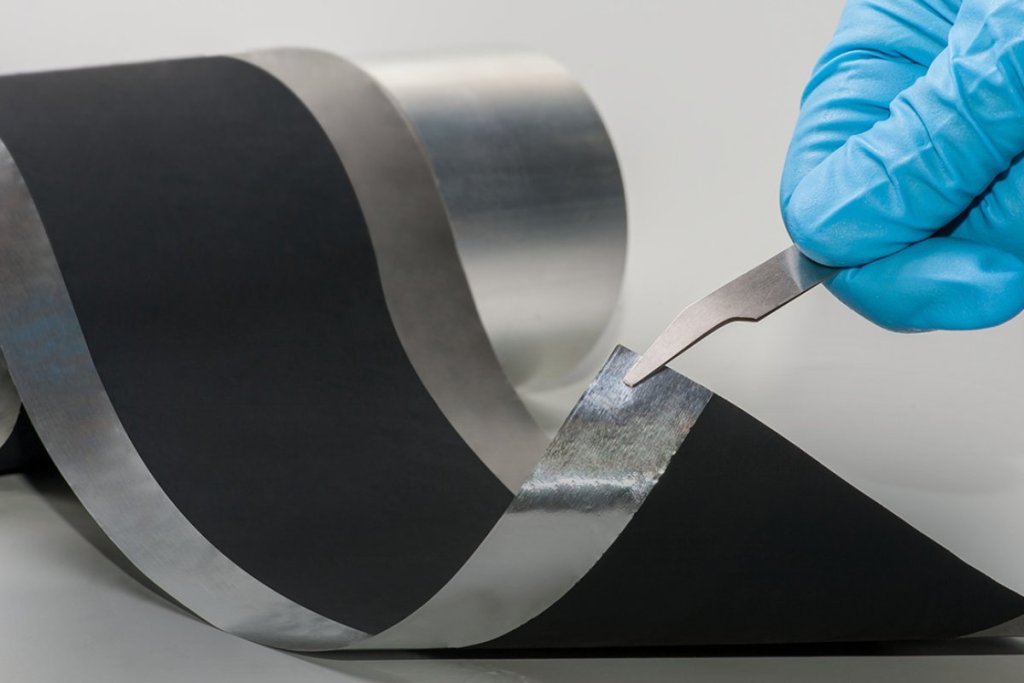
Eddy Current Sensors for Inline Battery Collector Thickness, Defect & Ni Foam Characterization Non-contact. Inline. High precision at production speed. Our eddy current sensor systems enable real-time thickness, defect and gap measurement for copper and aluminum battery collectors – even at line speeds exceeding 100 m/min. The technology provides stable performance under high gap conditions, […]
Gas Diffusion Layer Testing for Fuel Cell Optimization
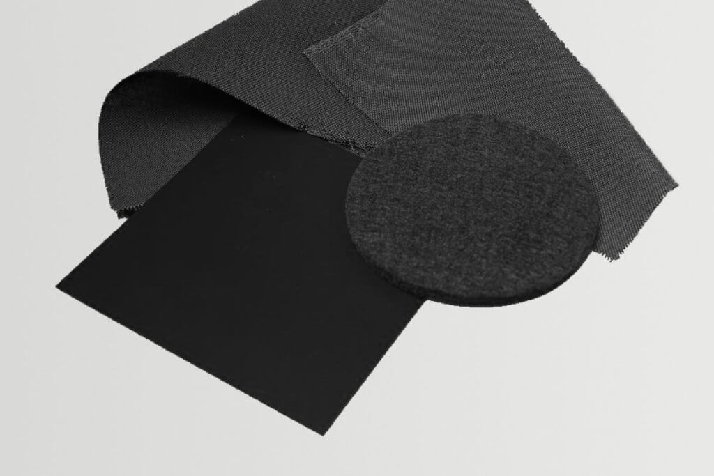
Gas Diffusion Layer Testing for Fuel Cell Optimization Background and Technical Context The gas diffusion layer (GDL) is a porous, electrically conductive material that plays multiple critical roles in fuel cell operation. Positioned between the bipolar plate and the catalyst layer, the GDL must simultaneously facilitate gas transport from the flow field channels to the […]
Quality Control of Catalyst Layers in Fuel Cell Production
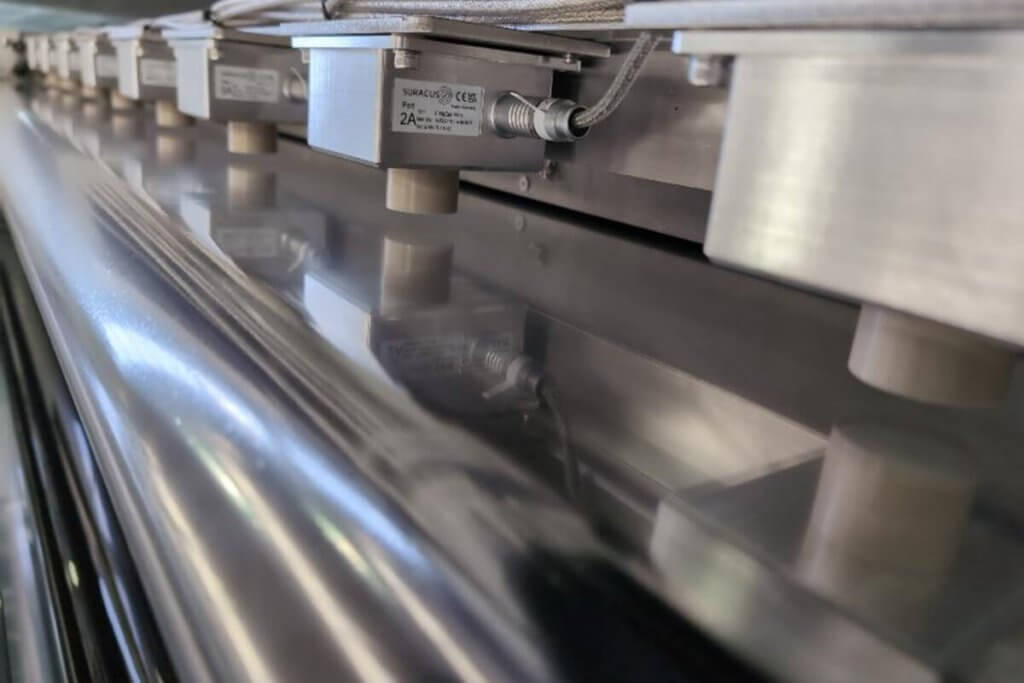
Quality Control of Catalyst Layers in Fuel Cell Production Background and Technical Context The catalyst layer represents the electrochemically active heart of a fuel cell, where the critical reactions that convert chemical energy into electrical energy occur. At the anode, hydrogen molecules are split into protons and electrons; at the cathode, oxygen combines with protons […]