CMP Process Monitoring and Endpoint Detection
Enabling Real Time Metal Film Thickness Measurement for Precision Planarization Control
Chemical Mechanical Planarization (CMP) is an indispensable process in modern semiconductor manufacturing, enabling the global planarization required for multilevel interconnect structures at advanced technology nodes. As device geometries shrink below 10 nm and interconnect layers exceed 20 levels, precise control of material removal during CMP has become critical to achieving acceptable yield and device performance.
Traditional time based polishing and optical endpoint detection methods struggle to meet the demands of copper and barrier metal CMP, where tight control of dishing, erosion, and within wafer uniformity is essential. In situ eddy current sensing provides a direct, non contact method to monitor metal film thickness in real time during the polishing process, enabling:
- Precise endpoint detection for copper, tungsten, and barrier metal CMP
- Real time removal rate monitoring for process control and uniformity optimization
- Zone specific thickness feedback for multi zone pressure adjustment
- Reduced over polishing to minimize dishing and erosion defects
SURAGUS high frequency eddy current sensors are engineered for integration into CMP equipment, operating reliably in the demanding wet environment while providing nanometer scale thickness resolution. This application note describes how in situ eddy current measurement addresses key CMP challenges and enables the process control required for advanced semiconductor manufacturing.
Table of Contents
Industry Context
The semiconductor industry’s relentless pursuit of smaller, faster, and more power efficient devices has driven dramatic increases in circuit complexity. Modern logic devices at the 5 nm node and below require 15 to 20 or more metal interconnect layers, while advanced 3D NAND memory stacks exceed 200 layers. Each of these layers requires precise planarization to enable subsequent lithography and deposition steps. Chemical Mechanical Planarization has emerged as the only technique capable of achieving the global and local planarity required for these advanced structures. The CMP equipment market has grown correspondingly, with applications expanding from traditional oxide and tungsten polishing to include copper dual damascene, barrier metals, low k dielectrics, and novel materials for advanced packaging. Key market drivers include:- Advanced logic scaling: FinFET and Gate All Around (GAA) transistors require precise gate height control
- 3D NAND expansion: increasing layer counts demand more CMP steps with tighter uniformity
- Advanced packaging: fan out wafer level packaging (FOWLP) and hybrid bonding require ultra flat surfaces
- New interconnect materials: cobalt, ruthenium, and molybdenum introduce new CMP challenges
The Role of In Situ Thickness Measurement
In situ metrology, measurement performed inside the process tool during operation, provides critical advantages over offline measurement for CMP control:| Aspect | Offline Metrology | In Situ Metrology |
|---|---|---|
| Feedback time | Minutes to hours | Real time (milliseconds) |
| Wafer sampling | Selected wafers only | Every wafer, every pass |
| Process adjustment | Next lot or wafer | Current wafer |
| Endpoint accuracy | Statistical estimate | Direct measurement |
| Over polish margin | Large (conservative) | Minimal (optimized) |
- Endpoint detection: identifying when the target film has been removed
- Removal rate monitoring: tracking polish rate in real time for SPC
- Uniformity control: providing zone specific feedback for multi zone heads
- Process optimization: enabling adaptive recipes based on incoming film thickness
CMP Process Overview
CMP Fundamentals
Chemical Mechanical Planarization combines chemical etching and mechanical abrasion to remove material from a wafer surface.
The process involves:
- Polishing pad: a porous polyurethane pad that provides mechanical action
- Slurry: a chemical solution containing abrasive particles and reactive chemicals
- Carrier head: holds and presses the wafer against the rotating pad
- Platen: supports the pad and provides rotation
During polishing, the rotating wafer is pressed face down against the rotating pad while slurry flows across the surface.
Chemical reactions soften the surface material, which is then mechanically removed by the abrasive action.
The combination of chemical and mechanical effects enables material removal rates and selectivities that neither mechanism could achieve alone.
┌─────────────────────────────────────────────────────────────┐ │ CMP SYSTEM SCHEMATIC │ │ │ │ Carrier Head │ │ (rotating) Slurry │ │ ┌───┐ Supply │ │ │ ◯ │ │ │ │ ┌────┴───┴────┐ ▼ │ │ │ Wafer │ ~~~~ │ │ │ (face down)│ │ │ └─────────────┘ │ │ ═══════════════════════════════════ ← Polishing Pad │ │ ┌─────────────────────────────────┐ │ │ │ Platen (rotating) │ │ │ └─────────────────────────────────┘ │ │ ▲ │ │ │ │ │ Sensor Window │ │ (for in situ measurement) │ └─────────────────────────────────────────────────────────────┘
Metal CMP Applications
Metal CMP processes are essential for creating the interconnect structures that carry signals and power throughout the integrated circuit:
Copper CMP (Dual Damascene)
The dominant interconnect metal for logic and memory devices, copper CMP involves:
- Bulk copper removal to expose the barrier layer
- Barrier removal (Ta or TaN) to expose the dielectric
- Buff polish to achieve final surface quality
Tungsten CMP
Used for contact plugs and local interconnects, tungsten CMP requires:
- High selectivity to underlying oxide
- Low dishing in wide features
- Minimal erosion in dense arrays
Barrier Metal CMP
Barrier layers (Ta, TaN, TiN, Co) require separate optimization due to:
- Very different polish rates versus copper
- Critical interface with low k dielectrics
- Impact on via resistance and reliability
Critical CMP Defects
Dishing
The over removal of soft metal (copper) relative to the surrounding harder dielectric, creating a concave depression in wide metal features.
Before CMP After CMP (with dishing)
┌────────────────────┐ ┌────────────────────┐
│▓▓▓▓▓▓▓▓▓▓▓▓▓▓▓▓▓▓▓▓│ │ │
│▓▓▓▓▓▓▓▓▓▓▓▓▓▓▓▓▓▓▓▓│ │ ╲ ╱ │
│▓▓▓▓▓▓▓▓▓▓▓▓▓▓▓▓▓▓▓▓│ │ ╲──────╱ │ ← Dishing
├────┬────────────┬───┤ ├────┬────────────┬───┤
│ │ Copper │ │ │ │ Copper │ │
│ │ │ │ │ │ │ │
│ │ │ │ │ │ │ │
└────┴────────────┴───┘ └────┴────────────┴───┘
Dielectric Dielectric
Erosion
The overall thinning of both metal and dielectric in high pattern density regions relative to low density areas.
Impact of these defects includes:
- Increased interconnect resistance (dishing)
- Reduced dielectric breakdown margin (erosion)
- Lithography focus issues in subsequent layers
- Via formation problems and opens
- Yield loss and reliability degradation
The Challenge: Limitations of Current Endpoint Methods
Time Based Polishing
The simplest approach uses fixed polish times based on historical removal rates. Limitations include:- No compensation for incoming thickness variation
- No adaptation to removal rate drift
- Requires large over polish margin for safety
- Results in excessive dishing and erosion
Motor Current and Torque Monitoring
Changes in friction between wafer and pad cause measurable changes in motor current. This method:- Provides whole wafer average signal only
- Cannot distinguish spatial variations
- Signal is indirect and affected by pad condition
- Low sensitivity for barrier clearing
Optical Endpoint Detection
Optical methods (reflectometry, interferometry) monitor light reflected from the wafer surface. Limitations include:- Interference from underlying pattern structures
- Sensitivity to slurry opacity and bubbles
- Window contamination and clouding
- Limited to materials with distinct optical properties
- Cannot measure absolute thickness
Summary of Limitations
| Method | Spatial Resolution | Absolute Thickness | Metal Sensitivity | Environmental Robustness |
|---|---|---|---|---|
| Time based | None | No | Not applicable | Not applicable |
| Motor current | Whole wafer | No | Low | Good |
| Optical | Single point | Limited | Moderate | Poor (slurry effects) |
| Eddy current | Single point | Yes | Excellent | Excellent |
The SURAGUS Solution: In Situ Eddy Current Sensing
Eddy Current Measurement Principle
When a high frequency alternating magnetic field is applied near a conductive material, eddy currents are induced within the conductor. These currents create their own magnetic field that opposes the original field, causing measurable changes in the sensor’s impedance. For thin conductive films, the magnitude of the eddy current response depends directly on the film’s sheet resistance, which is related to thickness by: Rs = ρ / t Where:- Rs = Sheet resistance (ohms per square)
- ρ = Material resistivity (ohm meter)
- t = Film thickness (meter)
Advantages for CMP Applications
| Advantage | Benefit for CMP |
|---|---|
| Non contact | No wear, no contamination of wafer |
| Insensitive to slurry | Reliable through opaque slurry |
| Direct thickness measurement | Absolute values, not just trends |
| High sensitivity to metals | Excellent for Cu, W, Co, barrier metals |
| Fast response | Real time monitoring at process speeds |
| Robust construction | Withstands wet, abrasive environment |
SURAGUS Sensor Technology
SURAGUS has developed specialized eddy current sensors optimized for CMP integration: EddyCus® Inline Sensors- Compact form factor for platen integration
- Sealed construction for wet environment operation
- Operating frequency optimized for target film thickness range
- High speed measurement capability (more than 50 readings per second)
| Parameter | Specification |
|---|---|
| Thickness range | 50 nm to 10 µm (material dependent) |
| Resolution | Less than 1 nm (under optimized conditions) |
| Measurement rate | Up to 50 Hz |
| Lift off tolerance | Up to 5 mm |
| Operating environment | Wet, 10 to 40°C |
| Output interface | Analog (0 to 10 V) or digital (RS485, Ethernet) |
Measurement Performance
Sensitivity Optimized coil geometry and electronics achieve measurement sensitivity greater than 2 mV per nm at typical CMP lift off distances (1.5 to 3 mm), enabling nanometer scale resolution. Repeatability System repeatability better than plus or minus 0.5 percent enables reliable detection of small thickness changes during polishing. Speed Measurement rates up to 50 Hz provide multiple data points per wafer rotation, enabling real time process monitoring and control. 
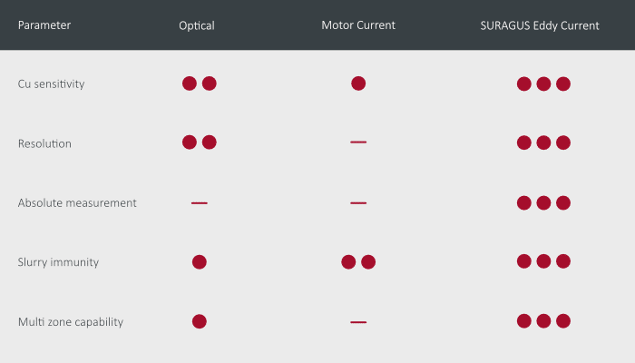
Comparison with Alternative Methods| Parameter | Optical | Motor Current | SURAGUS Eddy Current |
|---|---|---|---|
| Cu sensitivity | Moderate | Low | Excellent |
| Resolution | About 5 nm | Not applicable | Less than 1 nm |
| Absolute measurement | No | No | Yes |
| Slurry immunity | Poor | Good | Excellent |
| Multi zone capability | Limited | No | Yes |
Integration Architectures
Platen Integrated Configuration
The most common integration approach positions the sensor in the polishing platen, measuring through a window in the pad.
┌─────────────────────────────────────────────────────────────┐ │ PLATEN INTEGRATION │ │ │ │ Carrier Head (rotating) │ │ ┌─────────────┐ │ │ │ Wafer │ ←── Wafer face down │ │ └─────────────┘ │ │ ═══════════╤═════════════════════════ ← Polishing Pad │ │ │ Window │ │ ┌──────────┴──────────────────────────┐ │ │ │ Platen │ │ │ │ ┌──────────────┐ │ │ │ │ │ SURAGUS │ │ │ │ │ │ Eddy Current│ ←── Sensor in platen │ │ │ │ Sensor │ │ │ │ │ └──────┬───────┘ │ │ │ └────────────┼────────────────────────┘ │ │ │ │ │ ▼ │ │ Signal Processing │ │ & Data Output │ └─────────────────────────────────────────────────────────────┘
Measurement Geometry
As the platen rotates, the sensor passes under the wafer once per revolution.
The relative rotation of wafer and platen causes the sensor to trace a complex path across the wafer surface, sampling different radial positions on successive passes.
Advantages
- Measures actual wafer being polished
- Multiple zones sampled per rotation
- Minimal modification to carrier head
- Sensor protected below pad surface
Multi Sensor Configuration
For enhanced spatial resolution and faster feedback, multiple sensors can be distributed across the platen:
┌─────────────────────────────────────────────────────────────┐ │ MULTI SENSOR CONFIGURATION │ │ (Top View) │ │ │ │ ┌─────────────┐ │ │ │ Wafer │ │ │ │ │ │ │ ┌──●──────┼─────────────┼───────●──┐ │ │ │ S1 │ │ S2 │ ← Platen │ │ │ │ │ │ │ │ │ ●────┼─────────────┼────● │ │ │ │ S3 │ │ S4 │ │ │ │ │ │ │ │ │ └─────────┼─────────────┼──────────┘ │ │ │ │ │ │ └─────────────┘ │ │ │ │ S1 to S4: SURAGUS Eddy Current Sensors │ └─────────────────────────────────────────────────────────────┘
Benefits
- Faster coverage of wafer zones
- Independent monitoring of center and edge regions
- Enhanced uniformity feedback for multi zone heads
- Redundancy for continuous operation
Data Integration
SURAGUS sensors integrate with CMP equipment control systems through multiple interfaces:
Real Time Control Interface
- Analog output (0 to 10 V, 4 to 20 mA) for direct feedback
- Digital protocols (RS485, Ethernet IP, PROFINET)
- Trigger and synchronization inputs for coordinated measurement
Data Logging and Analysis
- Continuous thickness versus time recording
- Zone averaged uniformity calculation
- Removal rate trending and SPC
- Recipe correlation and optimization
Equipment Communication
┌─────────────────────────────────────────────────────────────┐ │ DATA FLOW ARCHITECTURE │ │ │ │ ┌─────────────┐ ┌─────────────┐ ┌─────────────┐ │ │ │ SURAGUS │ │ Equipment │ │ Factory │ │ │ │ Sensor │─────│ Controller │─────
│ Host │ │ │ │ System │ │ │ │ (MES) │ │ │ └─────────────┘ └──────┬──────┘ └─────────────┘ │ │ │ │ │ │ │ ▼ │ │ │ ┌─────────────┐ │ │ └────────────
│ APC AEC │ │ │ Real time │ System │ │ │ feedback └─────────────┘ │ │ │ │ │ ▼ │ │ Multi zone head │ │ pressure control │ └─────────────────────────────────────────────────────────────┘
Application Examples
Copper Bulk CMP Endpoint Detection
The Challenge
In copper dual damascene processing, the bulk copper removal step must stop precisely at the barrier layer.
Insufficient removal leaves copper shorts; excessive removal causes barrier thinning, dishing, and erosion.
Impact Without Proper Measurement
- Under polish: copper residue causes shorts between lines (yield killer)
- Over polish: dishing in wide features increases resistance; erosion in dense areas causes via resistance variation
SURAGUS Solution
The eddy current sensor monitors copper thickness in real time during polishing:
Copper Thickness vs. Polish Time
Thickness
(nm)
│
1000├────────────╲
│ ╲
800├ ╲
│ ╲
600├ ╲
│ ╲
400├ ╲
│ ╲
200├ ╲
│ ╲_____ Endpoint trigger
0 ├───────────────────────────────────────
Time
0 20 40 60 80 (seconds)
↑
Endpoint detected
The sensor detects the approach to barrier layer and triggers the endpoint, enabling:
- Precise stopping at target remaining thickness
- Compensation for incoming thickness variation
- Adaptation to removal rate drift
Results
- Endpoint accuracy: plus or minus 5 nm remaining copper
- Dishing reduction: 30 to 50 percent versus time based process
- Wafer to wafer uniformity: less than 2 percent (1σ)
Multi Zone Uniformity Control
The Challenge
Incoming copper film from electroplating exhibits center to edge thickness variation of 5 to 15 percent.
Without compensation, this non uniformity transfers directly to post CMP thickness variation.
Impact Without Proper Measurement
- Non uniform remaining copper across wafer
- Variable interconnect resistance affecting circuit timing
- Edge die yield loss
SURAGUS Solution
Multiple eddy current sensors provide zone specific thickness feedback to the multi zone carrier head:
┌─────────────────────────────────────────────────────────────┐ │ MULTI ZONE UNIFORMITY CONTROL │ │ │ │ Incoming Profile Adjusted Pressure │ │ │ │ ┌───────┐ ┌───────┐ │ │ / \ │ │ │ │ / \ ───│ │ Target │ │ / \ │ │ profile │ │ ───────────────── └───────┘ │ │ Edge Center Edge Uniform │ │ │ │ ┌──────────────────────────────────────────────────┐ │ │ │ │ │ │ │ Zone 1 Zone 2 Zone 3 Zone 4 │ │ │ │ (edge) (mid rad) (mid rad) (center) │ │ │ │ ↑ ↑ ↑ ↑ │ │ │ │ │ │ │ │ │ │ │ │ Sensor 1 Sensor 2 Sensor 3 Sensor 4 │ │ │ │ │ │ │ └──────────────────────────────────────────────────┘ │ │ │ │ Feedback loop adjusts zone pressures to equalize │ │ removal rates and achieve uniform final thickness │ └─────────────────────────────────────────────────────────────┘
Results
- Within wafer uniformity improvement: 40 to 60 percent
- Edge yield recovery: 1 to 2 percent additional good die
- Reduced reliance on incoming film specification
Barrier Metal Endpoint Detection
The Challenge
After copper removal, the Ta or TaN barrier layer must be removed with high selectivity to the underlying dielectric.
The barrier is thin (10 to 30 nm), making endpoint detection difficult.
Impact Without Proper Measurement
- Barrier residue causes via resistance issues
- Over polish damages low k dielectric
- Pattern dependent clearing creates uniformity problems
SURAGUS Solution
High sensitivity eddy current measurement detects the barrier layer transition:
Signal Response During Barrier Polish Signal (mV) │ 50├────╲ │ ╲ 40├ ╲___ Copper clearing │ ╲ 30├ ───────────── Barrier layer │ ╲ 20├ ╲___ Barrier clearing │ ╲ 10├ ───── Endpoint │ 0├───────────────────────────────────────Time Cu Polish Barrier Polish
The distinct signal profile for barrier metals enables:
- Detection of copper to barrier transition
- Monitoring of barrier removal progress
- Endpoint at barrier clearing
Results
- Barrier clearing endpoint accuracy: plus or minus 2 nm
- Dielectric loss reduction: 20 to 30 percent
- Via resistance uniformity improvement: 15 percent
Tungsten CMP Process Control
The Challenge
Tungsten CMP for contact plugs requires stopping precisely at the underlying oxide.
Tungsten and oxide have very different removal rates, making over polish highly detrimental.
Impact Without Proper Measurement
- Tungsten dishing increases contact resistance
- Oxide erosion affects subsequent layer topography
- Contact to contact resistance variation
SURAGUS Solution
Eddy current monitoring provides direct tungsten thickness measurement throughout the process:
- Real time removal rate calculation
- Endpoint detection at target remaining thickness
- Process optimization based on actual removal behavior
Results
- Tungsten dishing reduction: 25 to 40 percent
- Contact resistance uniformity: less than 5 percent (1σ)
- Process time optimization: 10 to 15 percent throughput improvement
Advanced Packaging CMP
The Challenge
Fan out wafer level packaging (FOWLP) and hybrid bonding require ultra flat surfaces with sub nanometer topography.
Copper redistribution layers (RDL) must be polished to precise thickness with minimal dishing.
Impact Without Proper Measurement
- Surface topography affects bonding quality
- Thickness variation impacts impedance matching
- Dishing creates voids in bonded interfaces
SURAGUS Solution
High resolution eddy current measurement enables:
- Final thickness control to plus or minus 10 nm
- Real time uniformity monitoring
- Adaptive polishing for die to die consistency
Results
- Surface planarity: less than 1 nm RMS in critical areas
- Thickness accuracy: plus or minus 10 nm across redistribution layer
- Bond void reduction: 50 percent improvement
Benefits Summary
Quality Improvement
In situ eddy current monitoring directly improves CMP output quality:| Metric | Improvement |
|---|---|
| Endpoint accuracy | plus or minus 5 nm versus plus or minus 50 nm (time based) |
| Dishing reduction | 30 to 50 percent |
| Erosion reduction | 20 to 35 percent |
| Within wafer uniformity | 40 to 60 percent improvement |
| Wafer to wafer uniformity | 50 to 70 percent improvement |
Yield Enhancement
- Edge die recovery: 0.5 to 2 percent additional good die per wafer
- Defect reduction: fewer shorts (under polish) and opens (over polish)
- Parametric yield: tighter resistance distributions
- Reliability improvement: reduced stress from over polishing
Productivity Gains
| Benefit | Impact |
|---|---|
| Reduced over polish margin | 15 to 25 percent shorter polish time |
| Fewer rework wafers | 50 to 80 percent reduction in re polish |
| Reduced test wafers | 30 to 50 percent fewer monitor wafers |
| Faster process development | 2 to 3 times faster recipe optimization |
Cost Reduction
| Category | Savings Mechanism |
|---|---|
| Consumables | Shorter polish means less slurry, longer pad life |
| Equipment utilization | Higher throughput per tool |
| Scrap reduction | Fewer out of spec wafers |
| Engineering efficiency | Data driven process optimization |
Process Intelligence
- Trend analysis: early detection of removal rate drift
- Consumable monitoring: correlation with pad and slurry condition
- Equipment health: identification of mechanical issues
- Process correlation: links between upstream deposition and CMP results
Implementation Guide
Feasibility Assessment
SURAGUS offers feasibility studies to evaluate sensor performance for specific applications:
Phase 1: Application Analysis
- Review of target materials and thickness ranges
- Assessment of integration requirements
- Definition of performance targets
Phase 2: Sample Measurement
- Bench top evaluation of sensor response
- Characterization of signal versus thickness relationship
- Assessment of lift off and environmental effects
Phase 3: Benefit Estimation
- Projected performance improvements
- ROI calculation based on yield and productivity gains
- Integration cost and timeline estimation
Implementation Phases
A phased approach minimizes risk while demonstrating value:
Phase 1: Offline Characterization (4 to 8 weeks)
- Install sensor in test configuration
- Correlate eddy current signal with reference metrology
- Develop signal processing algorithms
Phase 2: In Situ Monitoring (8 to 12 weeks)
- Integrate sensor into CMP platen
- Collect data during production polishing
- Validate endpoint detection capability
- Compare results with optical and time based methods
Phase 3: Closed Loop Control (12 to 16 weeks)
- Connect sensor output to equipment controller
- Implement endpoint triggering
- Enable multi zone feedback (if applicable)
- Optimize recipes based on real time data
Phase 4: Production Deployment
- Full integration with equipment control system
- Recipe certification and qualification
- Operator training
- Ongoing support and optimization
Support and Services
SURAGUS provides comprehensive support for CMP sensor integration:
Engineering Support
- Sensor selection and customization
- Integration design assistance
- Signal processing algorithm development
- Performance optimization
Training
- Sensor operation and maintenance
- Data interpretation and analysis
- Troubleshooting procedures
Ongoing Service
- Calibration and verification
- Preventive maintenance
- Software updates and enhancements
- Application support
Conclusion
As semiconductor manufacturing advances to smaller geometries and more complex structures, the demands on CMP process control intensify.
Traditional endpoint detection methods, time based polishing, motor current monitoring, and optical techniques, cannot provide the precision, reliability, and spatial resolution required for advanced metal CMP processes.
In situ eddy current sensing addresses these limitations by providing:
- Direct thickness measurement of copper, tungsten, and barrier metals
- Real time monitoring throughout the polishing process
- Robust operation immune to slurry opacity and environmental variations
- Zone specific feedback for uniformity optimization
- Nanometer scale resolution for precise endpoint detection
SURAGUS high frequency eddy current sensors are engineered specifically for integration into CMP equipment, delivering the measurement performance required for advanced semiconductor manufacturing.
By enabling precise endpoint detection and uniformity control, SURAGUS sensors help CMP equipment manufacturers and semiconductor fabs achieve higher yield, better device performance, and improved productivity.
The path to sub 10 nm technology nodes demands metrology solutions that can operate in situ, in real time, with the precision that advanced devices require.
SURAGUS eddy current technology provides that capability for metal CMP, enabling the planarization precision that makes advanced semiconductors possible.