With International Technology Roadmap for Semiconductors (ITRS) retiring and International Roadmap for Devices and Systems (IRDS) taking over charge to roadmap the present and future technologies for the next 15 years, there is greater focus to look far more than Beyond CMOS. The introduction of Hetergenous Integration Roadmap (HIR) emphasizes the need to build systems i.e., the integration of independently manufactured components into high-level modules and packages. These assemblies are expected to have significantly improved functionalities and operational performances. With SiP, 3D & 2D interconnects and wafer level packaging (WLP) identified as three major technology areas for heterogenous integration, advanced packaging in semiconductor manufacturing is evolving rapidly by addressing the key drivers:
Need to reduce the package size
Increased performance
Reduced cost
Higher yield
Easier die testing
Increased flexibility
Faster time-to-market
The 4 leading advanced packaging form factors – fan-out package, SoIC/ Chiplets, 3D TSV/ Interposer, Dual-sided SIPs – are expected to provide high-value solutions for the growing markets:
Mobile
IoT wearables
Automotive
Healthcare
Big data & computing
Aerospace & defense
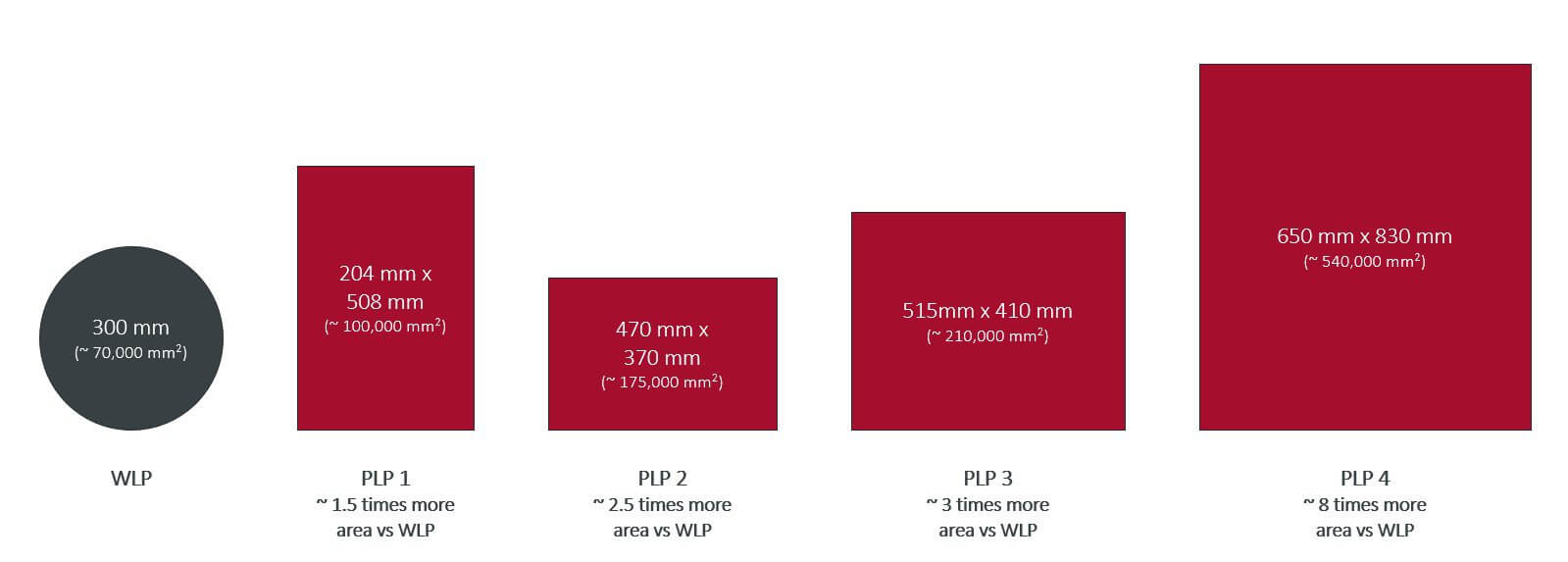
Besides technology developments towards heterogeneous integration, larger substrate formats are also considered. The current manufacturing capabilities on a wafer level goes up to 12″/300 mm. In order to target higher productivity and lower costs, larger form factors are targeted. Although 450 mm is the wafer level roadmap, it could be bypassed to approach panel level packaging (PLP), which might be the next big step. With immense potential to miniaturization and heterogenous integration, both technology approaches offer a lot of opportunities and benefits towards building high-performing systems. The PLP route is expected to follow the established standards in LCD and PCB manufacturing, thereby accelerating development and commercialization goals.
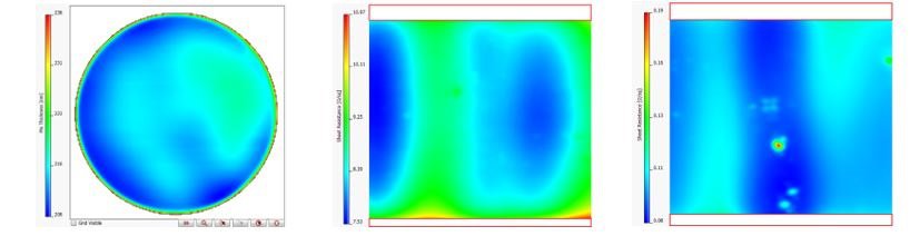
With more area in PLP, more dies are produced, eventually more devices and systems. The large-area metal deposition by PVD and ECD technologies in WLP and PLP are opening new avenues to in-line or offline thin-film characterization, especially by non-contact and non-destructive methods. For the high-throughput requirements, high frequency eddy current technology characterizes sheet resistance, conductivity, thickness and homogeneity of metal layers.
Left: Thickness imaging of Molybdenum on wafer, Center: Sheet resistance imaging of Titanium on glass for PLP, Right: Sheet resistance imaging of Copper on glass for PLP
Testing
Sheet resistance
Conductivity
Thickness
Homogeneity
Substrate Types
Wafer
Glass
Plastics (molded compounds)
Common Substrate Sizes
Wafer level
2 inch to 8 inch
Panel level
410 mm x 515 mm
510 mm x 515 mm
500 mm x 500 mm
600 mm x 600 mm
650 mm x 650 mm
Typical Layers
Cu
Ti
Processes
Plating
Sputtering
Evaporation
Testing Setups And Tools Portfolio
For wafer types Si, SiC, GaAs, GaN, glass, ceramic etc and for sizes 1” to 12”, SURAGUS’ full product portfolio includes manual single point tools, automated imaging tools and sensor integration kits for tool integration into existing or new tools.
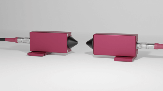
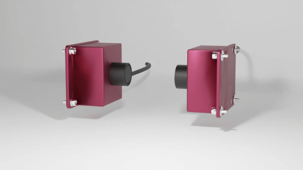
Sensor Integration For Process and Metrology Tools
Further Resouces
SEMI MF673 — Test Method for Measuring Resistivity of Semiconductor Wafers or Sheet Resistance of Semiconductor Films with a Noncontact Eddy-Current Gauge
SEMI M59 — Terminology for Silicon Technology
SEMI MF81 — Test Method for Measuring Radial Resistivity Variation on Silicon Wafers
SEMI MF84 — Test Method for Measuring Resistivity of Silicon Wafers with an In-Line Four-Point Probe
SEMI MF374 — Test Method for Sheet Resistance of Silicon Epitaxial, Diffused, Polysilicon, and Ion-Implanted Layers Using an In-Line Four-Point Probe with the Single-Configuration Procedure
SEMI MF1527 — Guide for Application of Certified Reference Materials and Reference Wafers for Calibration and Control of Instruments for Measuring Resistivity of Silicon