
Display
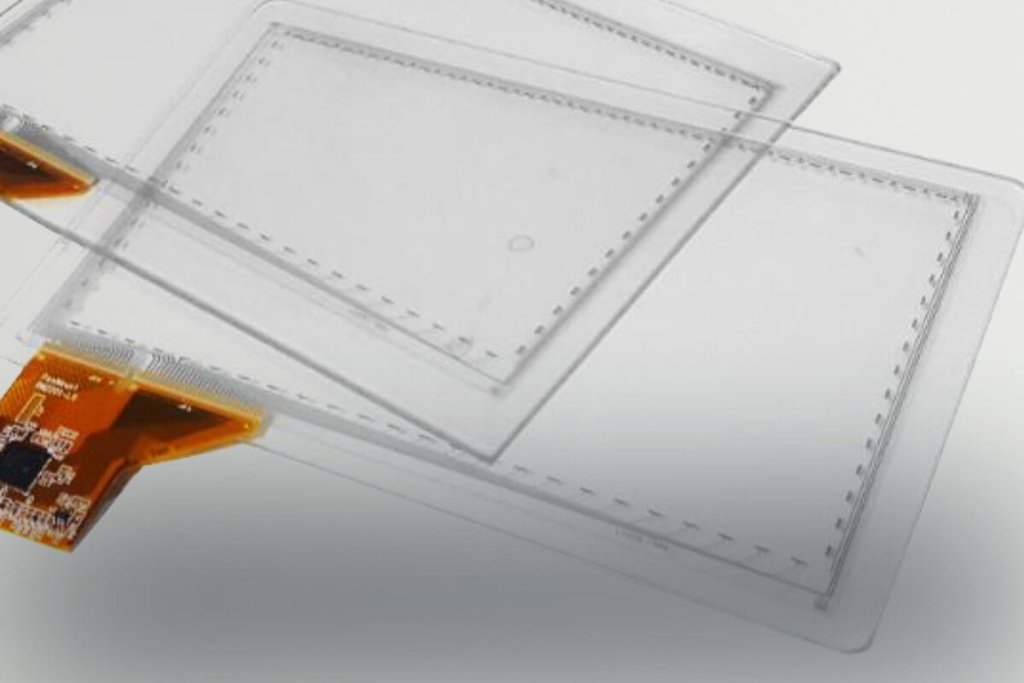
Measurement Solutions for Display Industry Touch Panel Sensor Front Panel Single Point Solutions Wafer Mapping Solutions SiC-Wafer Resistivity Homogeneity Si-Wafer Resistivity Homogeneity GaN-Wafer Resistivity Homogeneity GaAs-Wafer Resistivity Homogeneity Wafer Metallization Thickness Homogeneity Wafer Metallization Sheet Resistance Homogeneity Puck Slicing Quality Boules Crack and Defect Detection
Solar Industry
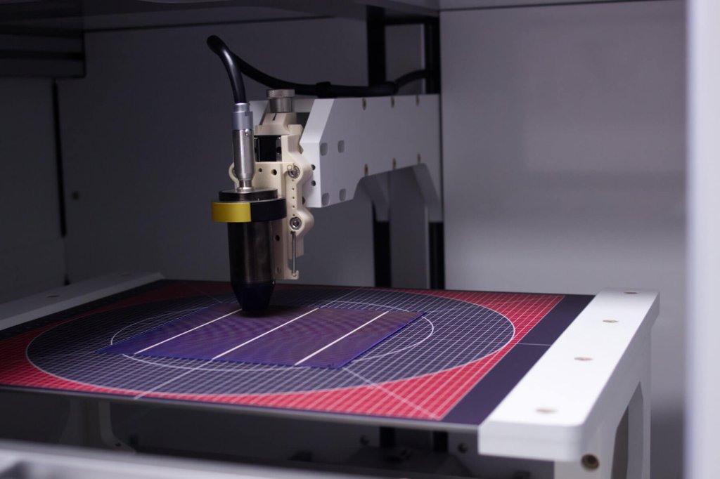
Measurement Solutions for the Solar Industry Process Monitoring Incoming silicon wafer inspection Deposition (PVD, CVD, etc.) Etching / polishing Doping Wet-processing Measurements Sheet resistance [Ω/□] Metal layer thickness [nm, µm] Resistivity [Ohm·cm] PN junction integrity testing Applications Wafer resistivity monitoring Sheet resistance monitoring of conductive layers (ITO at HJT) Metal layer thickness and sheet resistance […]
Printed Electronics Industry
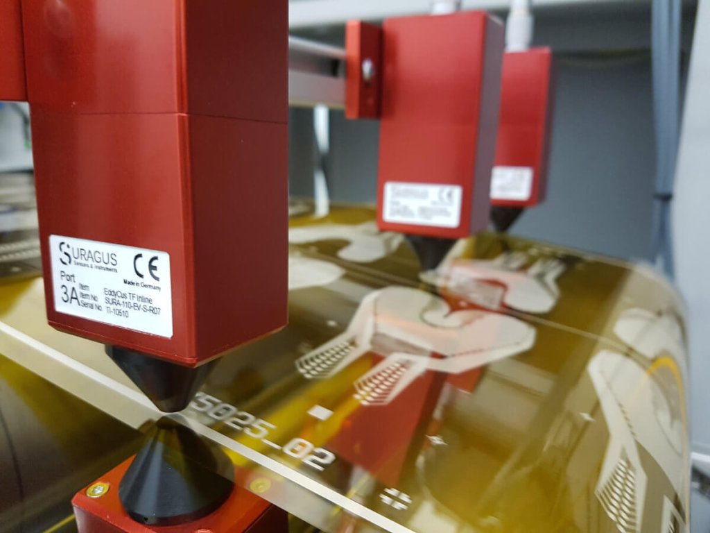
Measurement Solutions for Printed Electronics Applications Deposition processes (PVD, CVD, printing, curtain, slot die, spraying, etc.) Annealing / tempering processes Doping processes Drying Layer modification (removal etc.) Measurements Sheet resistance [Ohm/sq] Metal layer thickness [nm, µm] Optical transmittance / reflection Drying status Benefits Non-contact High accuracy High speed Solutions Portable EddyCus® portable Series Single Point […]
Glass Industry

Measurement Solutions for the Glass Industry Applications Deposition (PVD, CVD, etc.) Doping Annealing Tempering Layer removal Measurements Sheet resistance [Ohm/sq] Metal layer thickness [nm, µm, mil] Emissivity Optical densitiy / Transmittance / Reflectance / Haze Benefits Non-contact Highly accurate High sample rates Measurement of encapsulated layers Solutions Portable EddyCus® portable Handheld device for quick quality […]
Carbon Fiber Industry
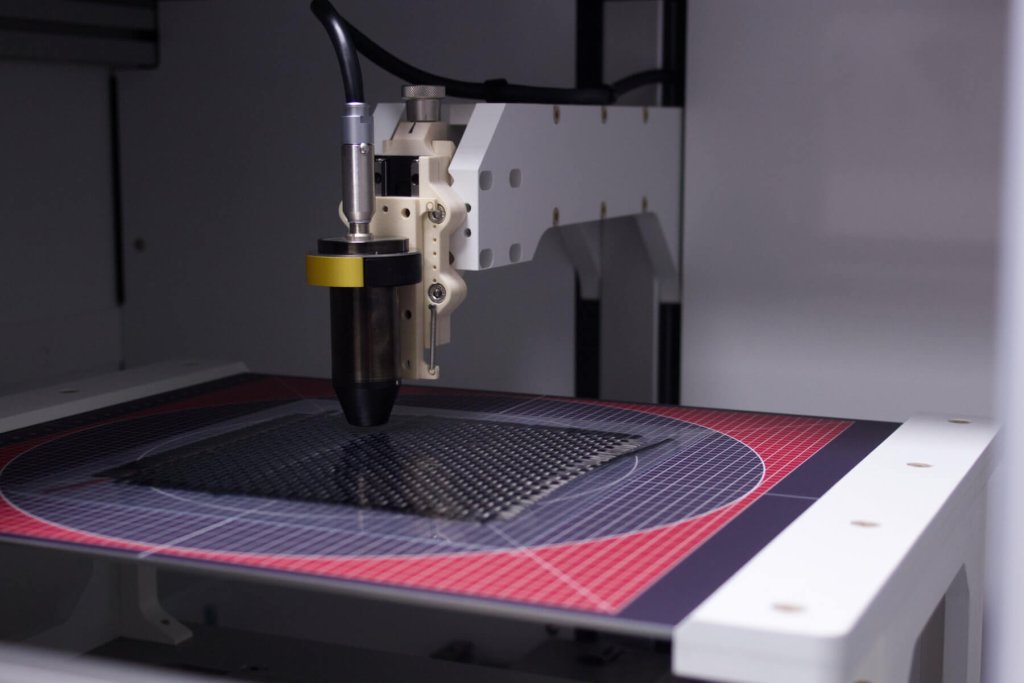
Measurement Solutions for Carbon Fiber Materials Applications Non-crimp fabrics (NCF) Preforms Multi-axial fabrics Roving, yarns and tows Carbon fiber reinforced plastics (CFRP) Carbon fiber stacks Carbon non-woven UD-tapes Damage and Defects Undulations and distortions Gaps Wrinkles and overlaps Misalignments Benefits Non-destructive Analyzation of hidden layer Imaging and inline solutions Characterizing Structural paramters such as Fiber […]
Fuel Cell Industry
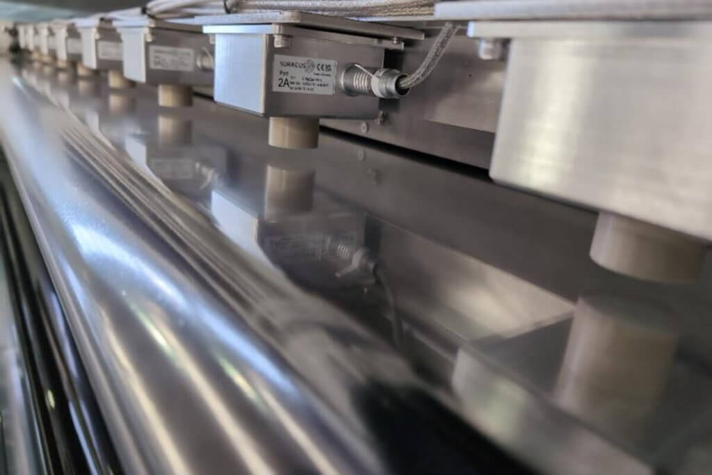
Measurement Solutions for Fuel Cell Industry Applications Membrane Electrode Assembly (MEA) Catalyst Coated Membrane (CCM) Gas Diffusion Layer (GDL) Bipolar Plates Deposition Processes (Extrusion, slurry deposition, doctoral blade) Drying Processes Degradation Monitoring Measurements Sheet Resistance [Ω/□] Metal Layer thickness [nm to µm] Coating Thickness [nm to µm] Coating Weight Distribution Thickness Homogeneity Mapping for Defects […]
Battery Industry
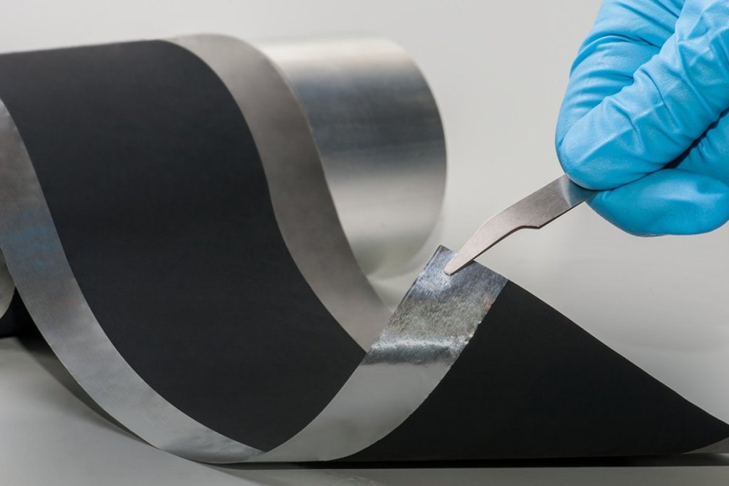
Measurement Solutions for Battery Industry Applications Slurry and Dry Batch Mixing Deposition Processes (Extrusion, Slurry Deposition, Doctoral Blade) Drying Processes Calendering Collector Coating Benefits Non-contact High Accuracy High Speed Measurements Sheet Resistance [Ω/□] Metal Layer Thickness [nm to µm] Carbon Black Content and Mixing Quality Binder Composition Coating Weight Distribution Thickness Homogeneity Residual Moisture Control […]
Semiconductor Industry
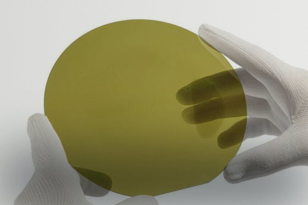
Measurement Solutions for Semiconductors Process Monitoring Deposition (PVD, CVD, etc.) Etching / Polishing Annealing / Tempering Doping / Implantation Defect monitoring Measurements Sheet Resistance [Ohm/sq] Metal Layer Thickness [nm, µm] Resistivity [Ohm·cm] Benefits Non-Contact High Sample Rate Imaging Solution Setups Benchtop Tools Tool Integration C2C Tools Solutions Single Point EddyCus® lab Series Imaging EddyCus® map […]