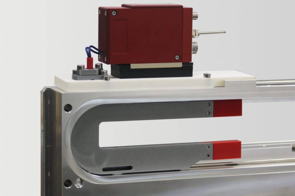
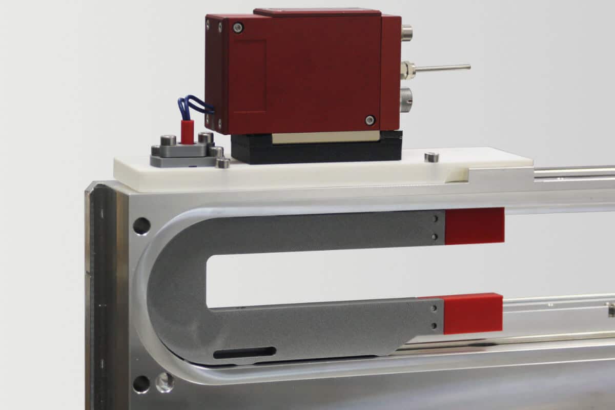
Sensor Capabilities
- Sheet Resistance [0.001 – 1,000 Ohm/sq]
- Metal Layer Thickness [5 nm – 2 mm]
- Resistivity [0.1 – 100 mOhm·cm]
Integration Points
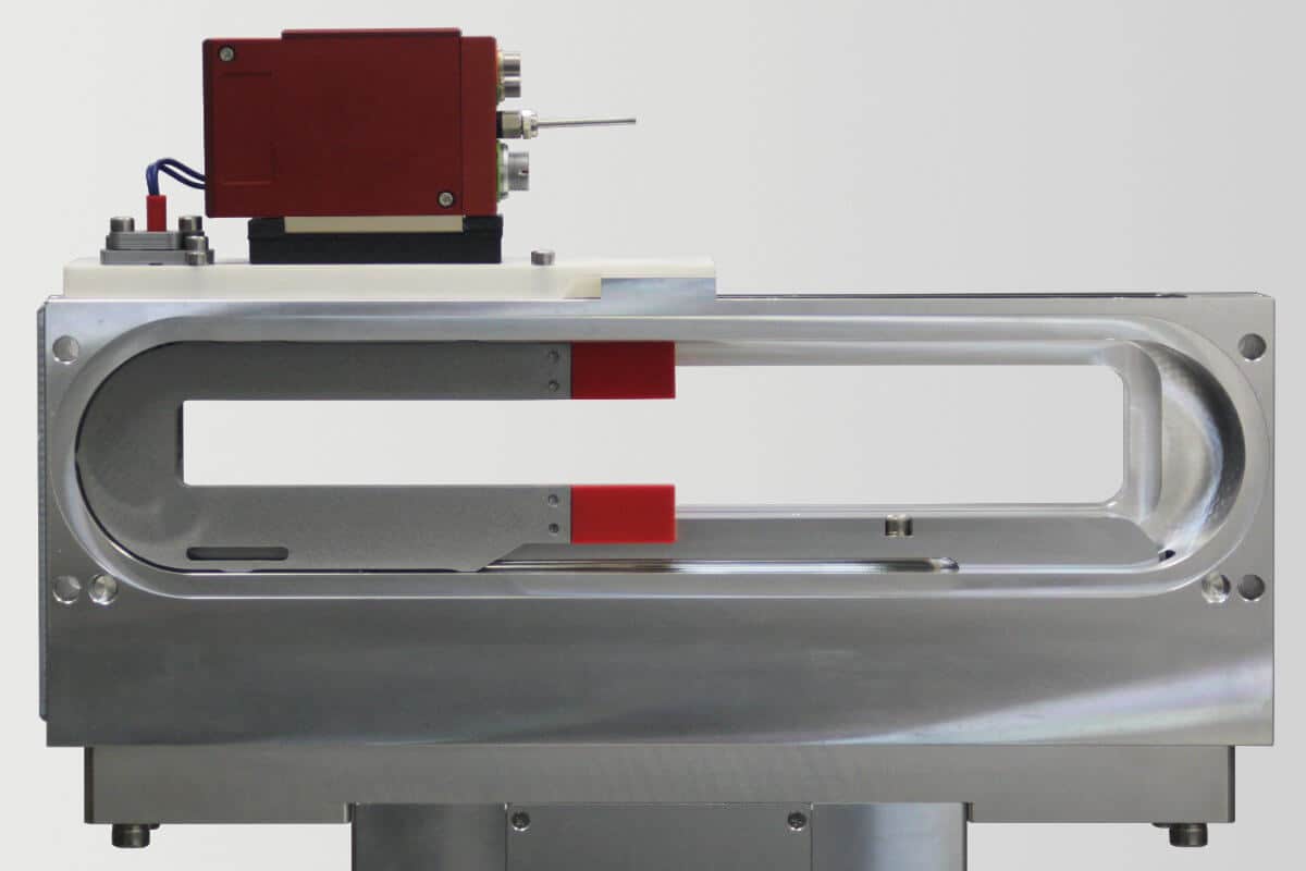
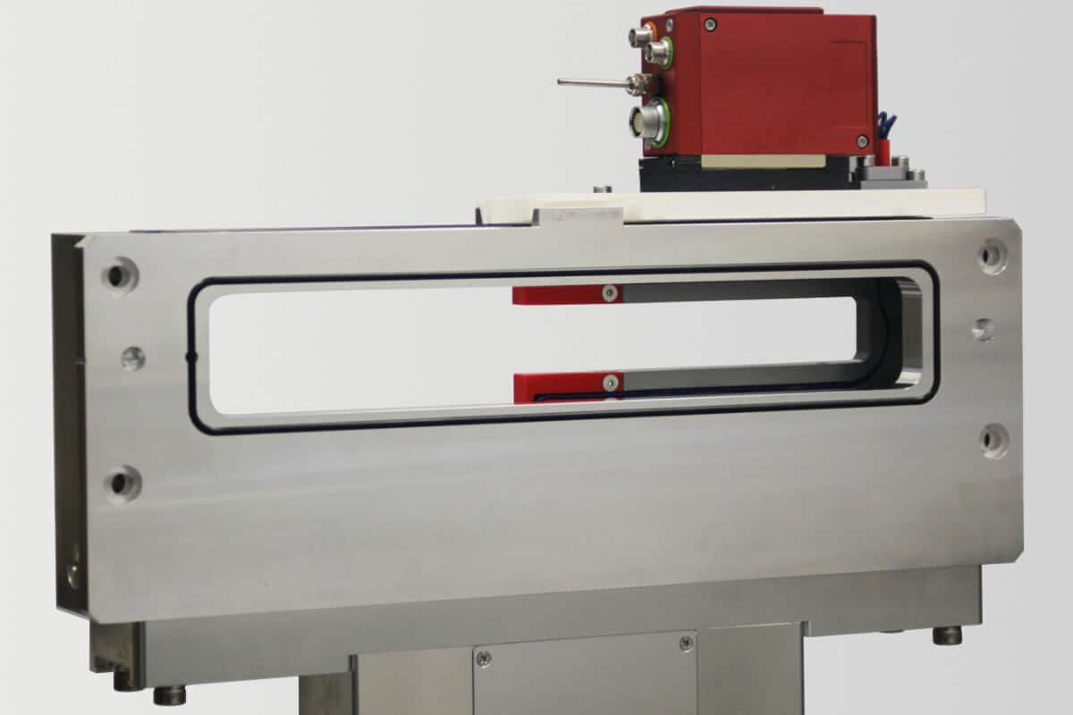
Semi-conformal in-vac feedthroughs such as
- Valves
- Ports
- Links
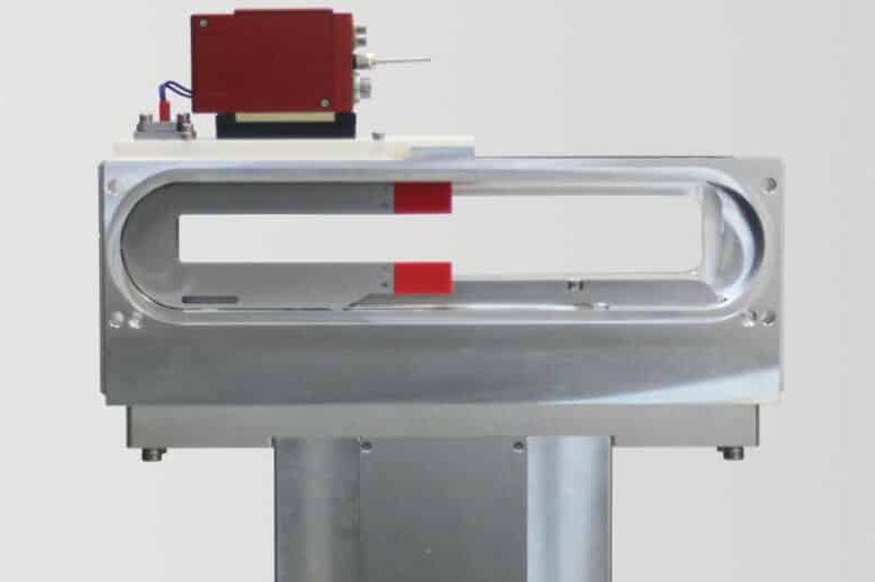
Supported Substrates
- 150 mm,
- 200 mm and
- 300 mm wafer
(Si, SiC, etc.)
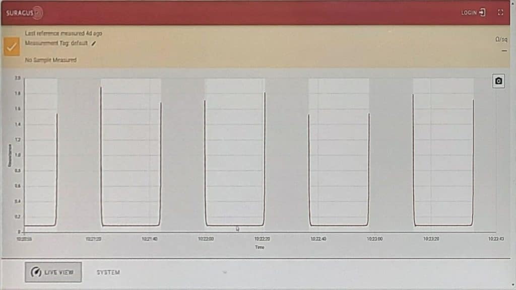
Data Extraction
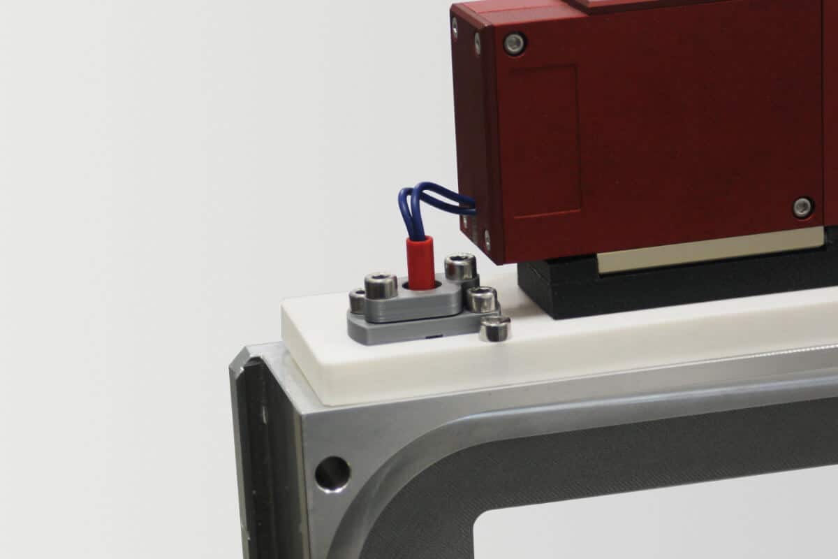
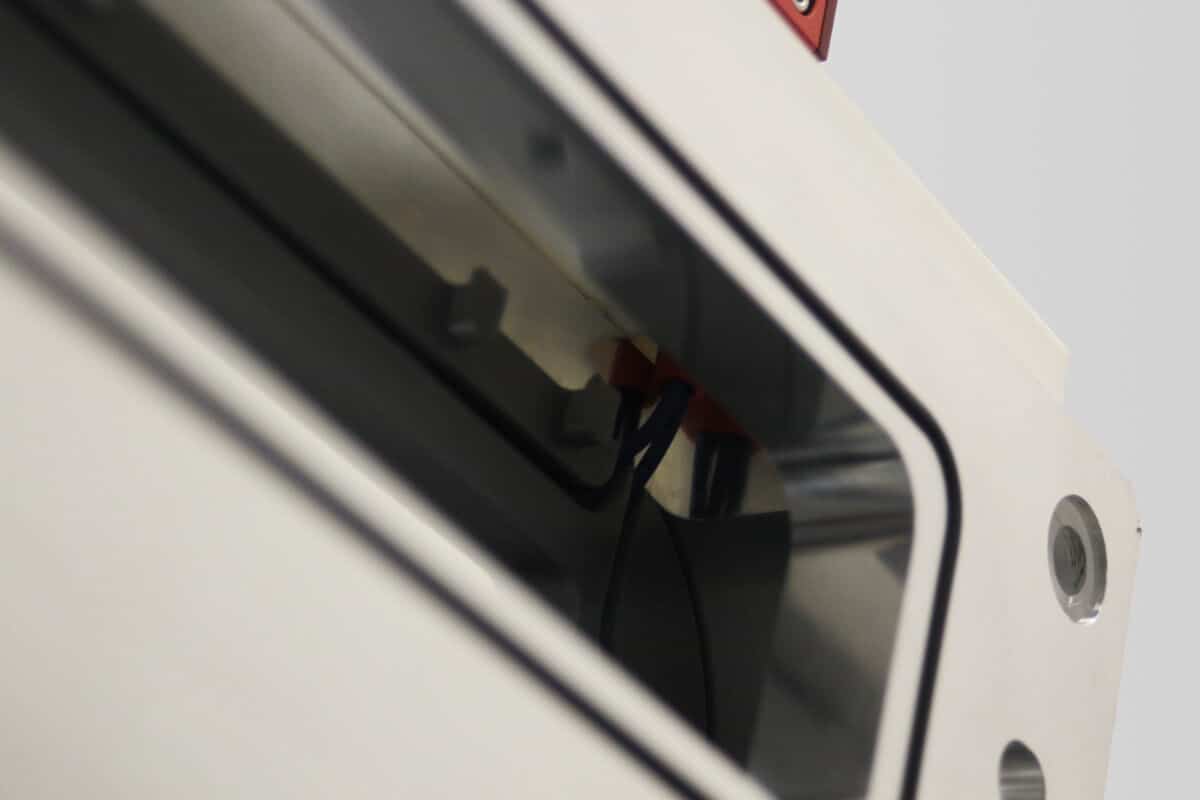
Data transmission runs through a dedicated lid
with a vacuum rated feedthrough that
connects the sensor to the control unit
Supported Interfaces
- UDP
- TCP
- Rest-API
- Modbus
- Profinet
- Analog/digital