Wafer Characterization

Semiconductor wafer substrates must meet strict specifications for resistivity, homogeneity, and structural integrity before they enter device fabrication. High-frequency eddy current technology provides a fast, contact-free method for characterizing bare and processed wafers — delivering the data needed to qualify incoming material, monitor crystal growth and wafering processes, and ensure substrate quality at every stage of the supply chain.

Testing Options in Wafer Characterization

Sheet resistance, expressed in ohms per square (Ω/sq), describes the lateral electrical resistance of the wafer material. Eddy current sensors determine this value without mechanical contact, making them suitable for fragile or polished wafer surfaces. The measurement serves as a rapid indicator of doping uniformity and substrate conductivity across the full wafer area.

Sheet Resistance

Sheet resistance, expressed in ohms per square (Ω/sq), describes the lateral electrical resistance of the wafer material. Eddy current sensors determine this value without mechanical contact, making them suitable for fragile or polished wafer surfaces. The measurement serves as a rapid indicator of doping uniformity and substrate conductivity across the full wafer area.

Wafer Resistivity

Bulk resistivity is a fundamental property of the wafer substrate, directly reflecting doping concentration and crystal quality. Eddy current measurement provides fast, non-destructive resistivity mapping that replaces or complements traditional four-point probe methods — with the advantage of zero surface contact and higher throughput.

Wafer Thickness

Precise wafer thickness data is critical for downstream processing, mechanical handling, and device performance. Eddy current sensors measure substrate thickness with high resolution, detecting variations introduced during crystal slicing, lapping, or polishing steps.

Wafer Homogeneity

Resistivity and thickness uniformity across the entire wafer surface directly impact device yield and performance consistency. Full-area eddy current mapping reveals radial and azimuthal variations in substrate properties, providing crystal growers and wafer manufacturers with actionable data to optimize their processes.

Permeability

For wafer substrates with magnetic properties — or to detect unwanted magnetic contamination — eddy current technology can assess permeability non-destructively. This is particularly relevant for specialty substrates used in sensor and MEMS applications where magnetic behavior affects device function.

Defectoscopy

Structural defects in the wafer substrate such as micro-cracks, voids, inclusions, or local resistivity anomalies can cause device failures downstream. Eddy current defectoscopy detects these flaws early — enabling sorting and grading of wafers before they enter costly fabrication steps.

Facette Formation

During crystal growth of materials like SiC or GaN, facets can form on the boule surface that propagate into sliced wafers, creating local variations in electrical properties. Eddy current characterization maps these facette-related inhomogeneities, supporting crystal growth optimization and wafer grading.

Wafer Bow & Warp

Bow and warp describe the geometric deformation of a wafer substrate — bow refers to the concave or convex curvature at the center, while warp captures the overall deviation from a perfectly flat plane. These parameters are critical for lithography compatibility and wafer handling in automated equipment. Eddy current-based measurement systems can detect thickness variations that correlate with bow and warp, providing complementary data to optical flatness tools and helping to identify substrates that risk chucking failures or focus errors during exposure.

Electrical Anisotropy

Electrical anisotropy describes the directional dependence of resistivity within the wafer substrate. It is particularly relevant for SiC wafers with off-axis crystal orientations, where the current flow differs along and perpendicular to the crystal c-axis. Eddy current technology can detect and quantify this anisotropy non-destructively, revealing crystal orientation effects, internal stress, and growth-related inhomogeneities that would remain invisible to scalar resistivity measurements alone.

Applications for Wafer Characterization

From incoming wafer inspection to full-area substrate mapping — eddy current characterization serves a wide range of workflows in wafer manufacturing and qualification.

Incoming Wafer Inspection

Before wafers enter device fabrication, incoming inspection verifies that the substrate material meets the required resistivity range, thickness tolerance, and homogeneity specifications. Eddy current measurement performs this check rapidly and without risk of surface damage, catching out-of-spec wafers before costly processing begins.

Wafer Imaging & Near Edge Monitoring

Advanced mapping systems generate full-area resistivity and thickness images of the wafer substrate. Near-edge monitoring extends the measurement coverage close to the wafer rim, capturing the peripheral zones where crystal growth and wafering processes often introduce the largest property variations.

Wafer Process Monitoring

Integrating eddy current sensors into the wafer manufacturing line — after slicing, lapping, polishing, or annealing — enables real-time tracking of substrate properties throughout the wafering process. Deviations from target specifications are detected immediately, reducing scrap and tightening process control.

Wafer Quality Control

As an integral part of wafer quality management, eddy current characterization delivers traceable measurement data that satisfies internal standards as well as industry norms such as SEMI MF673, SEMI MF81, and SEMI MF84. Results support certificate-of-conformance documentation and customer qualification requirements.

Wafer Deposition Process Control

Knowing the exact electrical properties of the bare wafer substrate is essential for calibrating and controlling subsequent deposition processes. Eddy current pre-characterization provides the baseline data that deposition tools need for accurate feed-forward process adjustments.

Pre- and Post-Treatment Process Control

Wafer substrates undergo various treatments — cleaning, annealing, surface preparation — that can alter their electrical and structural properties. Eddy current measurement before and after these steps quantifies the treatment effect and verifies that the wafer still meets its target specification.

Typical Wafer Substrates

Eddy current characterization covers the most important semiconductor wafer materials in use today.

Silicon (Si)

Silicon wafers remain the backbone of the semiconductor industry, used in integrated circuits, microprocessors, MEMS, sensors, and power devices. Grown by the Czochralski (CZ) method for standard applications or by Float Zone (FZ) for ultra-high-purity requirements, silicon substrates span a wide resistivity range — from heavily doped wafers below 0.005 Ω·cm to high-resistivity FZ material exceeding 10,000 Ω·cm. Eddy current metrology has been the standard for non-contact silicon wafer characterization for decades, delivering reliable resistivity and thickness data across all common wafer diameters.

Diameter Typical Thickness Resistivity Range Typical Applications
100 mm (4″) 525 ± 25 µm 0.001 – 100 Ω·cm MEMS, R&D, sensors
150 mm (6″) 675 ± 25 µm 0.001 – 10,000 Ω·cm Power devices, RF (FZ)
200 mm (8″) 725 ± 25 µm 0.005 – 100 Ω·cm IC, analog, MEMS
300 mm (12″) 775 ± 25 µm 0.005 – 50 Ω·cm Advanced logic, memory

Silicon Carbide (SiC)

SiC wafers are essential for power electronics, electric vehicle inverters, and high-temperature applications. The material’s wide bandgap, high thermal conductivity, and extreme hardness set it apart from silicon — but that same hardness makes contact-based probing risky and favors non-contact eddy current measurement. SiC substrates are available as n-type conductive wafers for vertical power devices or as semi-insulating material for RF and high-frequency components. The industry is transitioning from 150 mm to 200 mm wafers, driven by cost-per-die reduction goals.
Diameter Typical Thickness Resistivity Range Typical Applications
100 mm (4″) 350 ± 25 µm 0.01 – 0.05 Ω·cm (n-type) R&D, legacy power devices
150 mm (6″) 350 ± 25 µm 0.01 – 0.05 Ω·cm (n-type) SiC MOSFETs, diodes, EV inverters
150 mm (6″) 500 ± 25 µm > 10⁵ Ω·cm (semi-insulating) RF, microwave, 5G
200 mm (8″) 525 ± 25 µm 0.01 – 0.05 Ω·cm (n-type) Next-gen power electronics

Gallium Nitride (GaN)

GaN substrates and GaN-on-foreign-substrate wafers serve high-frequency, LED, and power device applications. Native GaN substrates are still comparatively small and expensive, so GaN epitaxy on silicon, sapphire, or SiC carriers remains the dominant approach for volume production. Eddy current technology characterizes the bulk electrical properties of the wafer stack, helping to assess crystal quality, doping uniformity, and substrate suitability for epitaxial growth.

Substrate Type Typical Diameter Typical Thickness Resistivity Range
Native GaN (free-standing) 50 – 100 mm 350 – 400 µm 0.01 – 0.05 Ω·cm (n-type)
GaN-on-Si 150 – 200 mm 675 – 1,150 µm Depends on Si carrier
GaN-on-SiC 100 – 150 mm 350 – 500 µm Semi-insulating SiC carrier
GaN-on-Sapphire 50 – 150 mm 330 – 650 µm Insulating carrier

Sapphire (Al₂O₃)

Sapphire wafers are widely used as carrier substrates for GaN-based LEDs and optical components. While sapphire itself is an electrical insulator, eddy current measurement remains relevant for characterizing the conductive layers in substrate stacks, detecting property variations introduced during crystal growth, and verifying wafer thickness and geometric uniformity. Sapphire’s optical transparency and chemical inertness also make it attractive for sensor and optical window applications.

Diameter Typical Thickness Resistivity Typical Applications
50.8 mm (2″) 330 ± 25 µm Insulating (> 10¹¹ Ω·cm) R&D, small-format LEDs
100 mm (4″) 500 – 650 µm Insulating LED epitaxy, optical windows
150 mm (6″) 650 ± 25 µm Insulating High-volume LED production

Wafer Characterization Across Process Steps

Wafer manufacturing involves a series of precisely controlled process steps — from crystal growth to final polishing. Eddy current wafer characterization can be applied between or during these steps to verify substrate quality, detect process-induced changes, and provide real-time feedback for optimization.
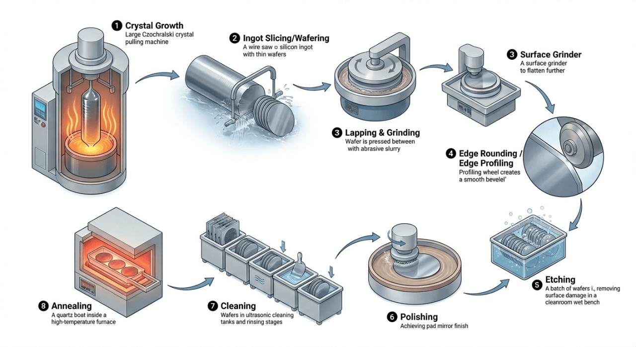
Crystal Growth

The wafer production chain begins with crystal growth — Czochralski (CZ) or Float Zone (FZ) for silicon, Physical Vapor Transport (PVT) for SiC, and HVPE or ammonothermal methods for GaN. The resulting boule already determines key substrate properties such as resistivity, doping uniformity, and defect density. Eddy current wafer characterization of boule slices and seed-end/tail-end wafers provides early feedback on crystal quality before committing to full downstream processing.

Ingot Slicing / Wafering

The grown crystal ingot is sliced into individual wafers using wire saws or ID saws. This step introduces mechanical stress, thickness variations, and potential sub-surface damage. Eddy current wafer characterization immediately after slicing detects thickness non-uniformity and resistivity shifts across the wafer, enabling early sorting and grading of as-cut substrates.

Lapping & Grinding

Lapping and grinding reduce wafer thickness to the target value and improve flatness by removing saw marks and sub-surface damage from slicing. Eddy current wafer characterization can monitor thickness and uniformity in real time during these steps, ensuring that the substrate approaches its target specification before moving to finer surface treatment.

Edge Rounding / Edge Profiling

Edge grinding and profiling shape the wafer rim to prevent chipping and improve handling in automated equipment. While this step primarily affects geometry, eddy current near-edge measurements can verify that the edge treatment has not introduced localized resistivity changes or micro-damage in the peripheral zone of the wafer.

Etching

Chemical etching removes the remaining sub-surface damage layer left by lapping and grinding. Depending on the etchant and process parameters, etching can also affect surface resistivity and wafer geometry. Eddy current wafer characterization before and after etching quantifies the material removal and verifies that the substrate’s electrical properties remain within specification.

Polishing (CMP / SSP / DSP)

Chemical-mechanical polishing (CMP) produces the mirror-smooth, epi-ready surface finish required for device fabrication. Wafers may be polished on one side (SSP) or both sides (DSP). Eddy current wafer characterization after polishing confirms final thickness, thickness uniformity (TTV), and resistivity — serving as the last quality gate before the wafer is shipped or enters epitaxy.

Cleaning

Multi-step wet cleaning sequences (e.g. RCA clean) remove metallic, organic, and particulate contaminants from the wafer surface. While cleaning itself does not alter bulk electrical properties, eddy current wafer characterization can detect residual metallic contamination through localized resistivity anomalies, providing a complementary check to particle inspection tools.

Annealing

Thermal annealing is used to activate dopants, reduce crystal defects, or adjust oxygen precipitation in silicon wafers. These treatments can significantly change the wafer’s resistivity profile. Eddy current wafer characterization before and after annealing reveals the spatial impact of the thermal process and ensures that the target resistivity distribution has been achieved.
Manufacturing Process Step
Wafer Characterization Checkpoint
1
Crystal Growth
CZ, FZ (Si) · PVT (SiC) · HVPE (GaN) — Boule growth defines base resistivity, doping and defect density.
Wafer Characterization
Measure: Resistivity, homogeneity, facette position (SiC)
Why: Qualify crystal doping & uniformity before committing to wafering
2
Ingot Slicing / Wafering
Wire saw or ID saw — Cuts boule into individual wafers. Introduces thickness variation and sub-surface damage.
Wafer Characterization
Measure: Thickness, thickness variation (TTV), resistivity
Why: Detect saw-induced variations for early sorting & grading of as-cut wafers
3
Lapping & Grinding
Reduces thickness to target, improves flatness, removes saw damage.
Wafer Characterization
Measure: Thickness, flatness, uniformity
Why: Verify target thickness is reached & material removal is even across wafer
4
Edge Rounding / Edge Profiling
Shapes wafer rim to prevent chipping and improve automated handling.
5
Etching
Chemical etch removes remaining sub-surface damage. May affect surface resistivity and geometry.
Wafer Characterization
Measure: Resistivity (pre/post), thickness change
Why: Quantify etch removal & confirm electrical properties remain in spec
6
Polishing (CMP / SSP / DSP)
Produces mirror-smooth, epi-ready surface finish for device fabrication.
Wafer Characterization
Measure: Final thickness, TTV, resistivity, bow & warp
Why: Last quality gate — confirms wafer meets all specs before shipment or epitaxy
7
Cleaning
RCA clean and multi-step wet cleaning — removes metallic, organic, and particulate contamination.
Wafer Characterization
Measure: Resistivity mapping (localized anomalies)
Why: Detect residual metallic contamination that cleaning may have missed
8
Annealing
Thermal treatment to activate dopants, reduce defects, or adjust oxygen precipitation.
Wafer Characterization
Measure: Resistivity distribution (pre/post anneal)
Why: Verify dopant activation & confirm target resistivity profile is achieved
Qualified Wafer - Ready for Shipment or Epitaxy
Substrate meets all specifications for resistivity, thickness, homogeneity, and structural integrity.

Wafer Characterization Integration

Eddy current wafer characterization integrates into diverse manufacturing architectures — from standalone lab tools and load lock chambers to fully automated inline inspection systems.

Wafer Level

Single-wafer characterization is performed in laboratory or quality-control settings using semi-automated or fully automated mapping systems. These wafer characterization tools scan the entire substrate surface and generate detailed property maps that reveal radial gradients, local anomalies, and overall uniformity.

Batch Systems

In batch wafering operations — where multiple wafers from the same boule or lot are processed together — eddy current wafer characterization monitors uniformity across the entire batch, ensuring wafer-to-wafer consistency after slicing, lapping, or annealing steps.

Load Lock

Load lock chambers manage wafer transfer between atmospheric and vacuum environments. Embedding eddy current sensors in the load lock enables wafer characterization between process steps without breaking vacuum, preserving throughput and process integrity.

Cluster Systems

Cluster tools connect multiple process chambers for sequential wafer treatment. Eddy current wafer characterization between chambers provides intermediate quality checks, catching property drift or anomalies before the substrate advances to the next process station.

Inline

For fully integrated production monitoring, eddy current sensors are installed directly in the manufacturing line. This enables real-time, wafer-by-wafer characterization during continuous operation — supporting 100% inspection without impacting throughput.

Environment

Eddy current wafer characterization adapts to the full range of measurement environments encountered in semiconductor wafer manufacturing — from vacuum chambers to atmospheric offline stations.

In-Vacuo and Ex-Vacuo

In-vacuo wafer characterization takes place directly inside a vacuum chamber, enabling substrate measurement during or immediately after high-temperature treatment without atmospheric exposure. Ex-vacuo wafer characterization is performed under ambient conditions — typically as part of offline quality control or incoming inspection routines.

In-Situ and Ex-Situ

In-situ wafer characterization is carried out at the point of process — for example during annealing or surface preparation — providing immediate feedback on how the treatment affects substrate properties. Ex-situ wafer characterization is performed at a separate metrology station, offering higher accuracy and repeatability for reference and qualification purposes.

Inline and Offline

Inline wafer characterization is embedded in the material flow and enables 100% substrate inspection in production. Offline wafer characterization is performed on sampled wafers at a dedicated station — ideal for in-depth analysis, process development, correlation studies, and customer qualification.

Wafer Characterization by Device Type

Eddy current wafer characterization supports a broad spectrum of semiconductor device segments — ensuring that the starting substrate meets the specific requirements of each end-use application.

Power Electronics

SiC and GaN wafers for power MOSFETs, IGBTs, and diodes require tightly controlled resistivity and crystal quality. Eddy current characterization ensures that substrate specifications are met before epitaxy and device fabrication begin.

Industry Electronics

Wafers destined for industrial electronic components must meet stringent reliability requirements. Substrate characterization by eddy current technology verifies material consistency and helps identify wafers that fall outside acceptable property ranges.

IC (Integrated Circuits)

The performance of integrated circuits depends on the uniformity of the starting wafer. Eddy current mapping provides full-area resistivity data that IC fabs use for wafer acceptance testing, bin sorting, and process feed-forward strategies.

MEMS

Micro-electromechanical systems are highly sensitive to substrate property variations. Eddy current characterization helps MEMS manufacturers select wafers with the right resistivity profile and uniformity level for their specific device requirements.

Microelectronics & Microprocessors

Advanced microprocessor nodes demand extremely uniform starting wafers. Eddy current metrology delivers the resolution and repeatability needed to qualify substrates for leading-edge logic and memory fabrication.

LED

Sapphire and GaN wafers for LED manufacturing must exhibit excellent crystallographic and electrical uniformity to ensure consistent luminous efficacy. Eddy current characterization supports substrate grading and incoming quality control for LED epitaxy lines.

Sensors

Semiconductor sensors for pressure, temperature, acceleration, and other physical quantities rely on precisely specified substrate properties. Eddy current measurement provides fast, non-destructive wafer qualification across the full range of sensor substrate materials.

Optics

Optical semiconductor devices — including photodetectors, laser diodes, and waveguides — require wafer substrates with tightly controlled electrical and structural properties. Eddy current characterization supports wafer selection and process qualification for optoelectronic manufacturing.

5G

Next-generation 5G RF components are built on GaN and SiC substrates that must meet demanding specifications for resistivity and crystal quality. Eddy current wafer characterization supports the qualification pipeline for power amplifiers and high-frequency modules used in mobile communications infrastructure.

Conclusion

Eddy current wafer characterization is an essential tool for the semiconductor substrate industry. It delivers precise, non-contact measurement of the electrical and structural properties that define wafer quality — from bulk resistivity and thickness to homogeneity and defect detection. With seamless integration into laboratory, cleanroom, and production-line environments, and full compatibility with Si, SiC, GaN, and sapphire substrates, eddy current metrology is positioned to grow alongside the industry’s expanding material and application landscape.