
Non-contact Resistivity Mapping System
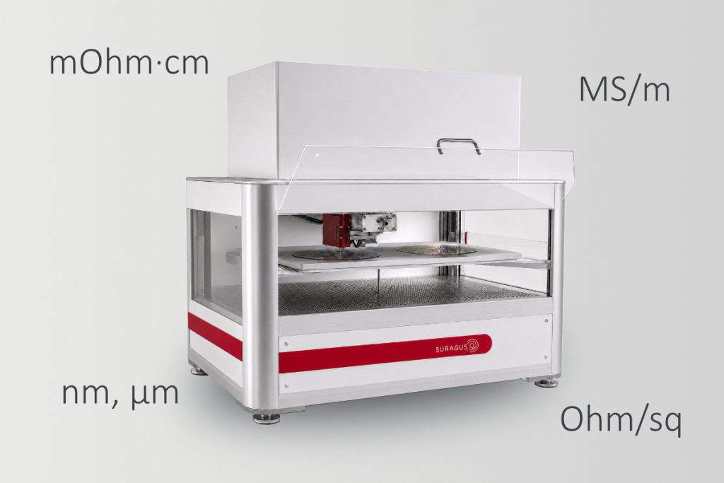
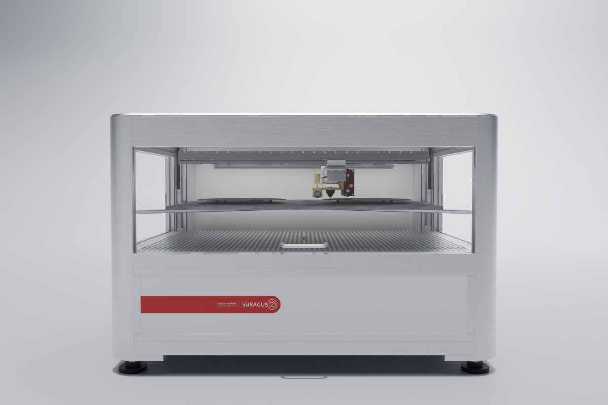
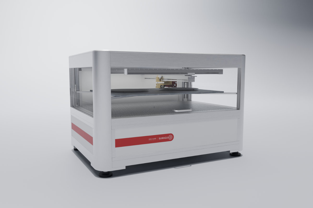
EddyCus® map 8060 RMT
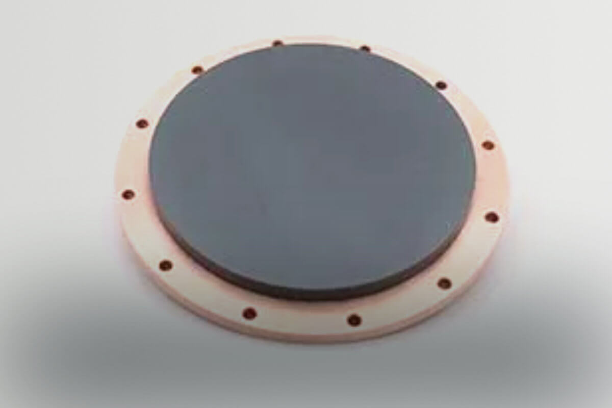
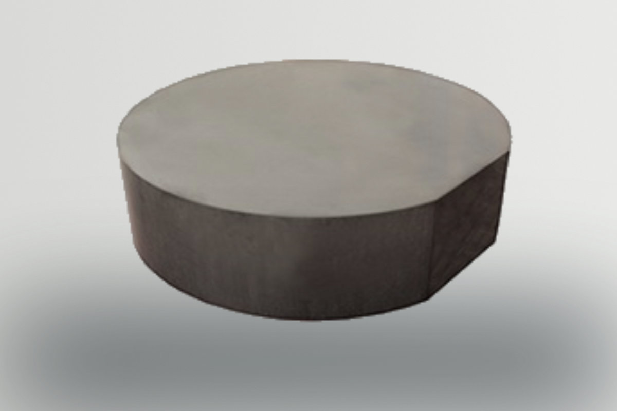
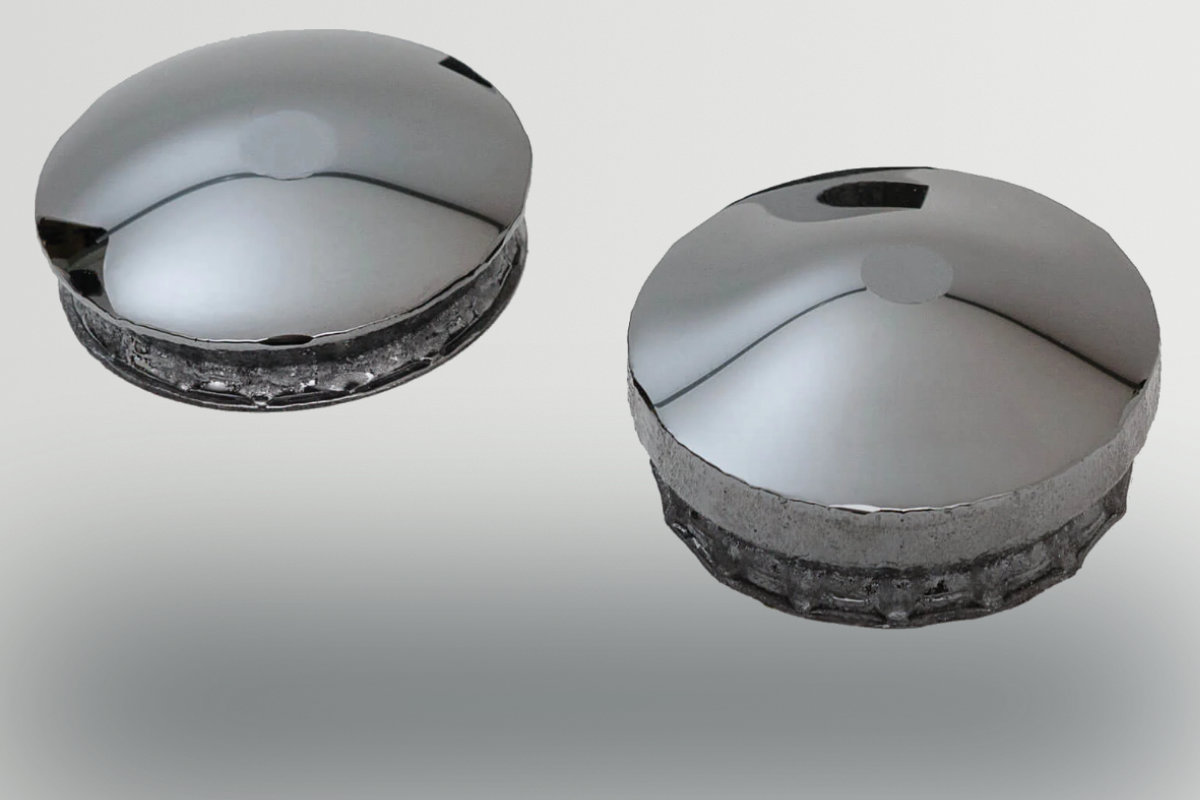
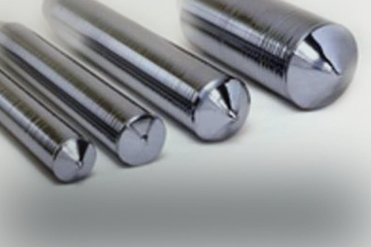
Resistivity and sheet resistance maps of samples up to 600 x 600 millimeter and 100 millimeter tall – boules, pucks, seeds and wafers on one tool, without contact and without sample preparation.
- Measurable area up to 600 mm x 600 mm
- Samples up to 100 mm tall, curved surfaces supported
- Valid data down to 1 mm from the sample edge
- Up to 70,000 measurement points per scan on a 300 mm wafer, scanning pitch from 1 mm
- Repeatability < 0.1 % (1σ)
- Process control with spatial uniformity data
Introduction
The EddyCus® map 8060 RMT measures the resistivity and sheet resistance of conductive samples up to 600 mm x 600 mm in non-contact mode. After manual placement of the sample, the system performs a fully automated scan and generates a high-resolution map across the entire surface. Because the eddy current sensor never touches the sample, there is no contact resistance, no probe damage and no sample preparation. Production material can be measured and then processed further.
The sensor takes readings while it travels across the sample rather than stopping at each point. Depending on the selected scanning pitch, users can prioritise short measurement times or high spatial resolution – up to 90,000 measurement points in a single scan. The resulting map resolves crystal facets, cracks, point defects and regions of differing crystalline type that a single-point measurement cannot detect.
Samples may be up to 100 mm tall and do not require a flat surface. With the adaptive Z-movement module, the sensor follows the topography of curved boules and pucks so that the working distance stays constant across the scan. With the Edge Effect Compensation module, valid data extends to within 1 mm of the sample edge instead of the 9 to 18 mm exclusion zone typical for eddy current measurements.
The device is typically used for:
- Incoming inspection of boules and ingots before wafering
- Doping uniformity control during crystal growth
- Facet and crystalline type mapping on pucks and seeds
- Wafer-to-wafer resistivity uniformity in production
- Edge region characterisation for yield analysis
- Incoming inspection of large-area coated panels and substrates
Features and Benefits
Sample Area up to 800 x 600 mm
Tall Samples up to 100 mm
Various Analyzing Options
Valid Data 1 mm from the Edge
Measurement on the Fly
Scanning Pitch Down to 1 mm
Easy to Use
Curved and Warped Surfaces
One Device, Multiple Measurement Parameters
The EddyCus® map 8060 RMT measures the electrical properties of the sample directly. Sheet resistance and resistivity are two views of the same measurement: with a known sample thickness, one converts into the other. Conductivity is the reciprocal of resistivity. Metal layer thickness is calculated from the measured sheet resistance and the known conductivity of the metal, which means the achievable thickness range follows directly from the sheet resistance range of the sensor. Sensor can be changed to adapt to different measurement tasks like high accuracy and repeatability resistivity or high spacial resolution.
- Resistivity
- Conductivity
- Sheet resistance
- Metal layer thickness
- Surface warp
- Bow
Software and Device Control
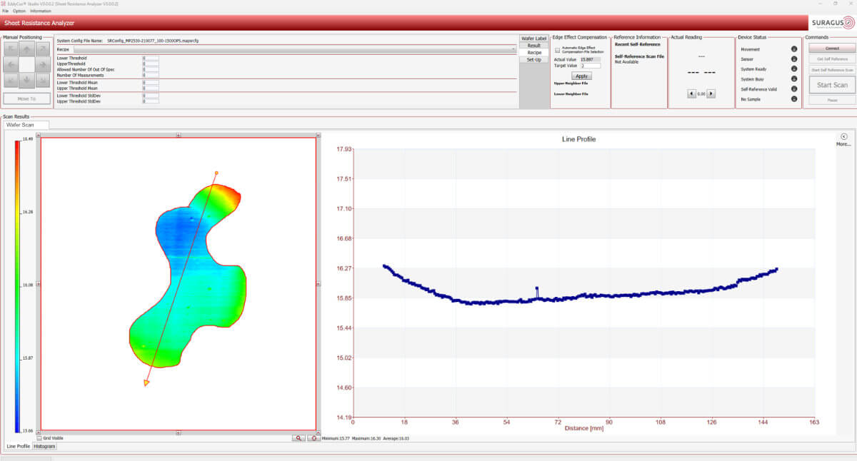
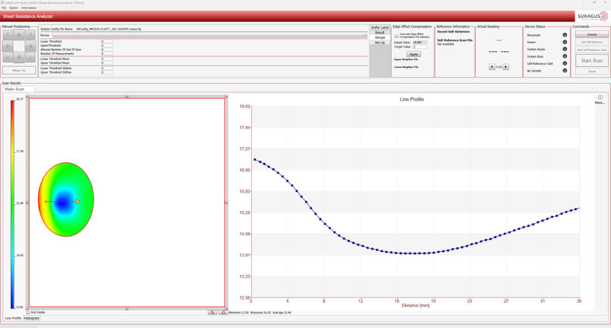
Operation: predefined measurement recipes for routine operation · recipe management with version control · full parameter access for application experts · real-time visualisation during the scan · multiple scan path options (meander, circular)
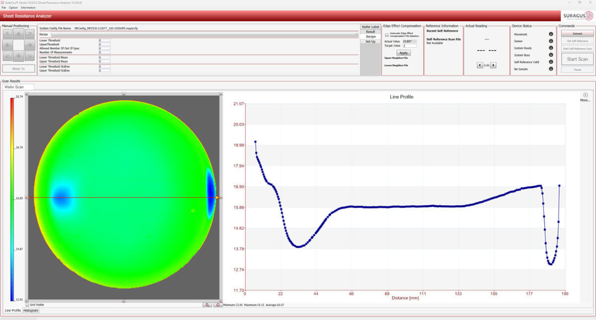
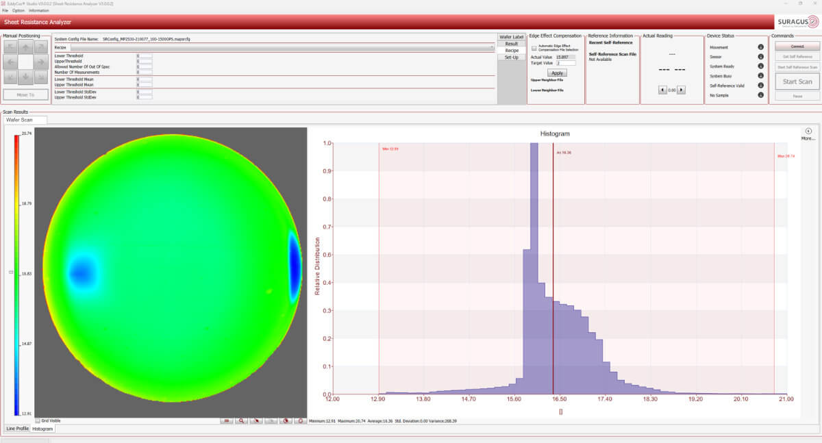
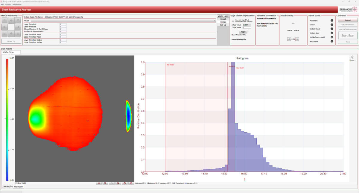
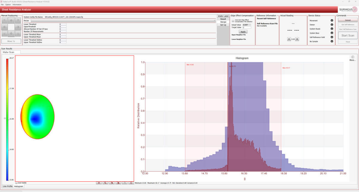
Analysis: 2D resistivity and sheet resistance mapping · statistical analysis (mean, standard deviation, uniformity) · line scan and profile extraction · histogram analysis, including within a freely selected area · single point analysis
Data management: InfluxDB time-series database · ASCII data export · automated PDF reporting with customisable templates
Data Table for EddyCus® map 8060 RMT
Device Features
| Measurement technology | Non-contact eddy current (reflection mode) |
| Sensor type | ASU Gen2 with fast trigger board |
| Max. trigger rate | 600 kHz |
| Effective data rate | 150 points per second |
| Repeatability | < 0.1 % (1σ) |
| Closed loop controlled working distance | 400 µm (≤ 6 mm depending on selected sensor) |
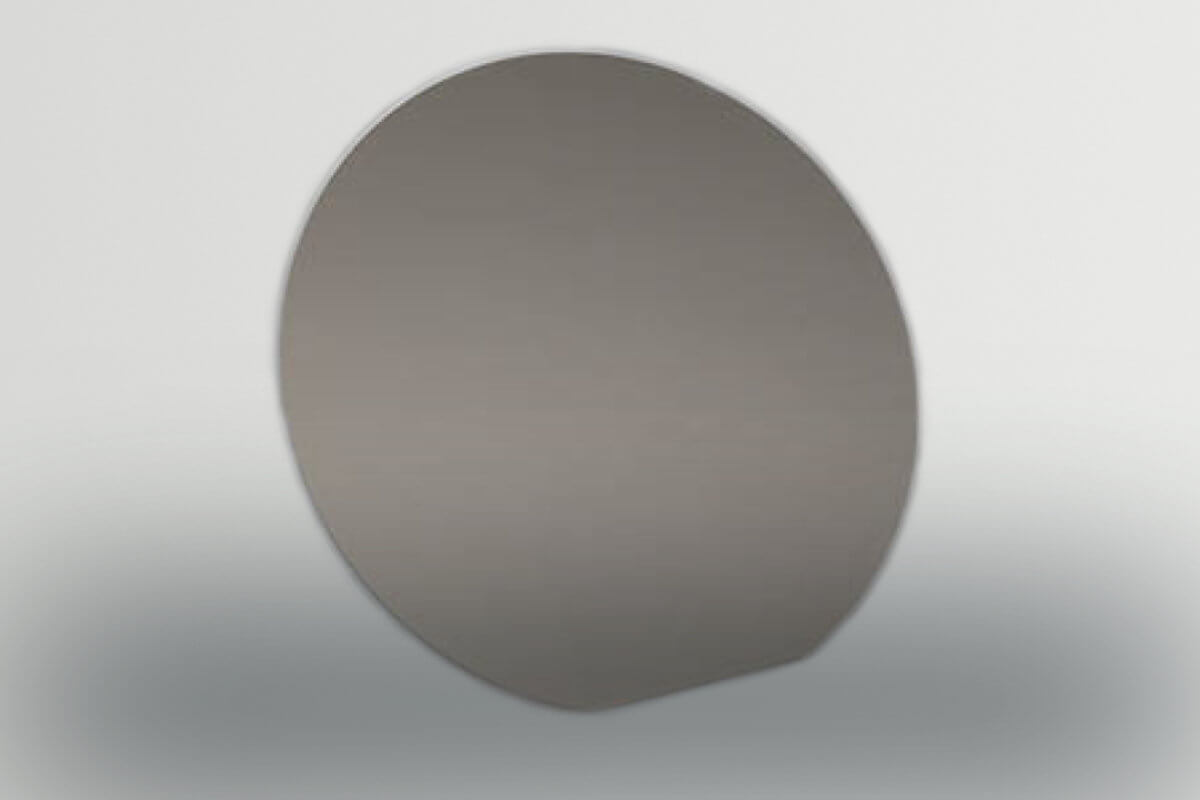
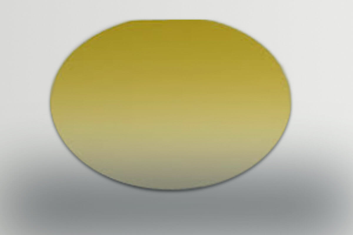
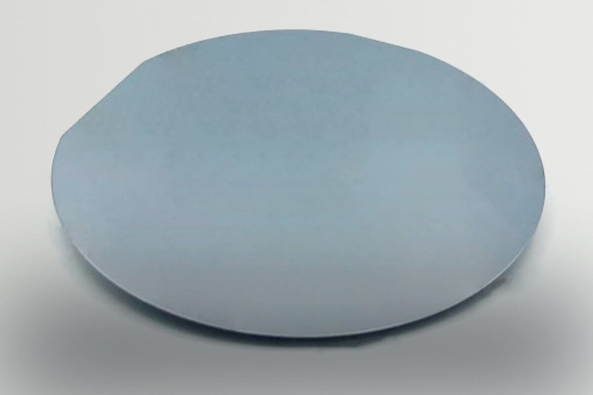
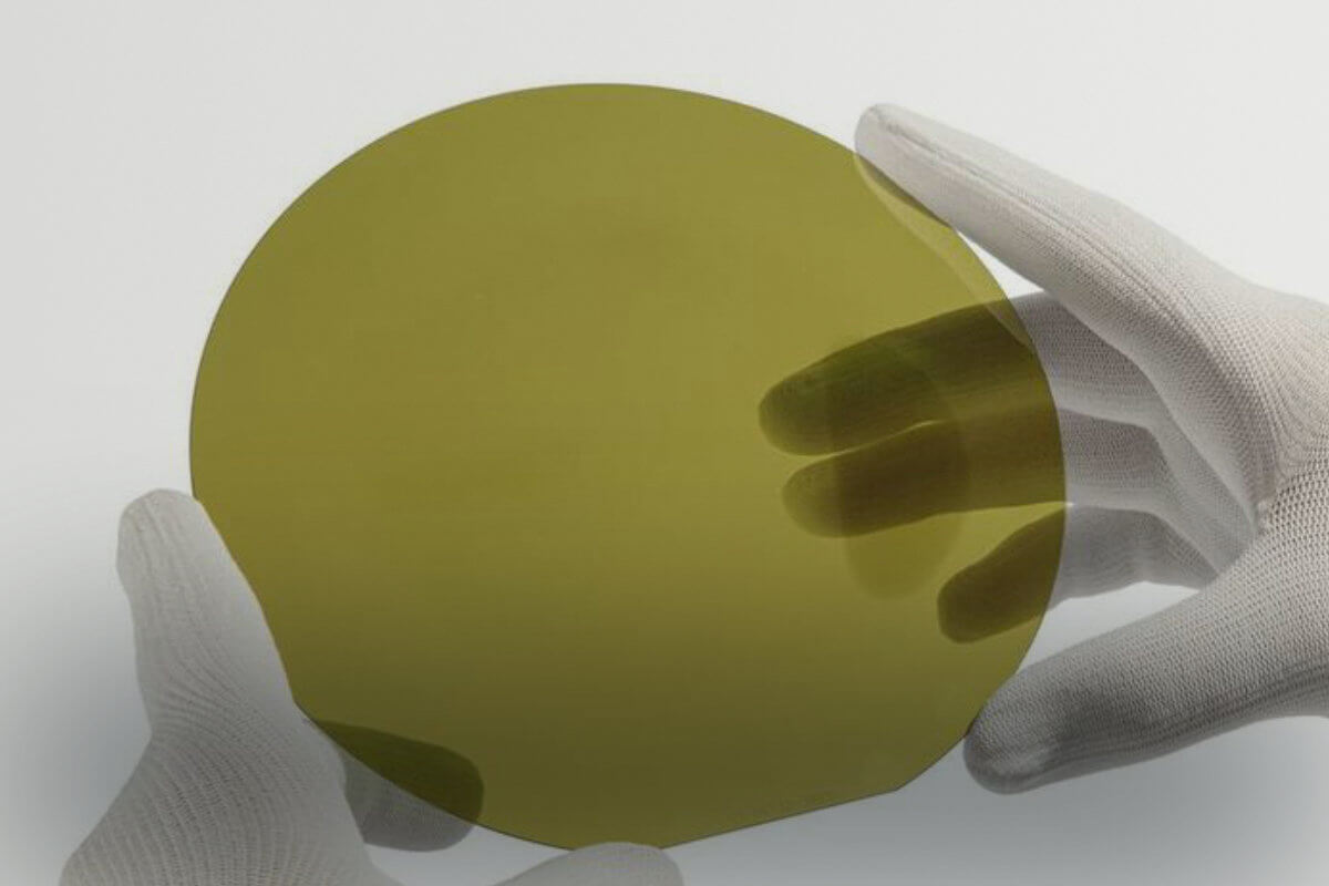
| Substrates | Seeds, ingots, boules, pucks, wafers and wafer parts |
| Sample area | 800 mm x 600 mm |
| Measurable sample area | 10 mm x 10 mm up to 600 mm x 600 mm (24 x 24 inch), larger upon request |
| Max. sample height | 100 mm |
| Edge effect correction / exclusion | 9 – 18 mm depending on resistivity; down to 1 mm with Module 9 (Edge Effect Compensation) |
| Scanning pitch | 1 / 2.5 / 5 / 10 / 25 mm |
| Measurement points per time | approx. 2,000 – 6,000 points per minute, depending on pitch and scan path |
| Scanning time (1 – 10 mm pitch) | 100 x 100 mm: 0.5 – 5 min 150 x 150 mm: 0.8 – 7.5 min 200 x 200 mm: 1 – 10 min 300 x 300 mm: 2 – 12 min |
| Axis travel range (X / Y / Z) | 800 mm / 600 mm / 150 mm |
| Positioning accuracy (X / Y / Z) | < ± 15 µm / < ± 15 µm / < ± 5 µm |
| Device dimensions (w/d/h) | max. 1090 mm x 799 mm x 670 mm |
| Weight | < 150 kg |
Measurement Capabilities
| Resistivity measurement | |
|---|---|
| Resistivity measurement range (standard sensor) | 1 – 50 mOhm·cm |
| Extended range with exchangeable sensors Sensor selection depends on the material and the targeted range |
Low 0.002 – 0.1 mOhm·cm Standard 0.1 – 100 mOhm·cm High 100 – 1,000 mOhm·cm |
| Sheet resistance measurement | |
| Sheet resistance measurement range (standard sensor) | 1 mOhm/sq – 100 Ohm/sq |
| Conductivity measurement | |
| Conductivity measurement range | 0.01 – 65 MS/m |
| Metal layer thickness measurement | |
| Metal thickness range Derived from the sheet resistance range. Values apply to copper. Accuracies depend on the selected setup and the type / conductivity of the metal (e.g. copper, aluminum, silver) (cf. our calculator) |
Low 1 – 10 nm; 2 – 5 % accuracy Standard 10 – 1,000 nm; 1 – 3 % accuracy High 1 – 17 µm; 0.5 – 3 % accuracy |
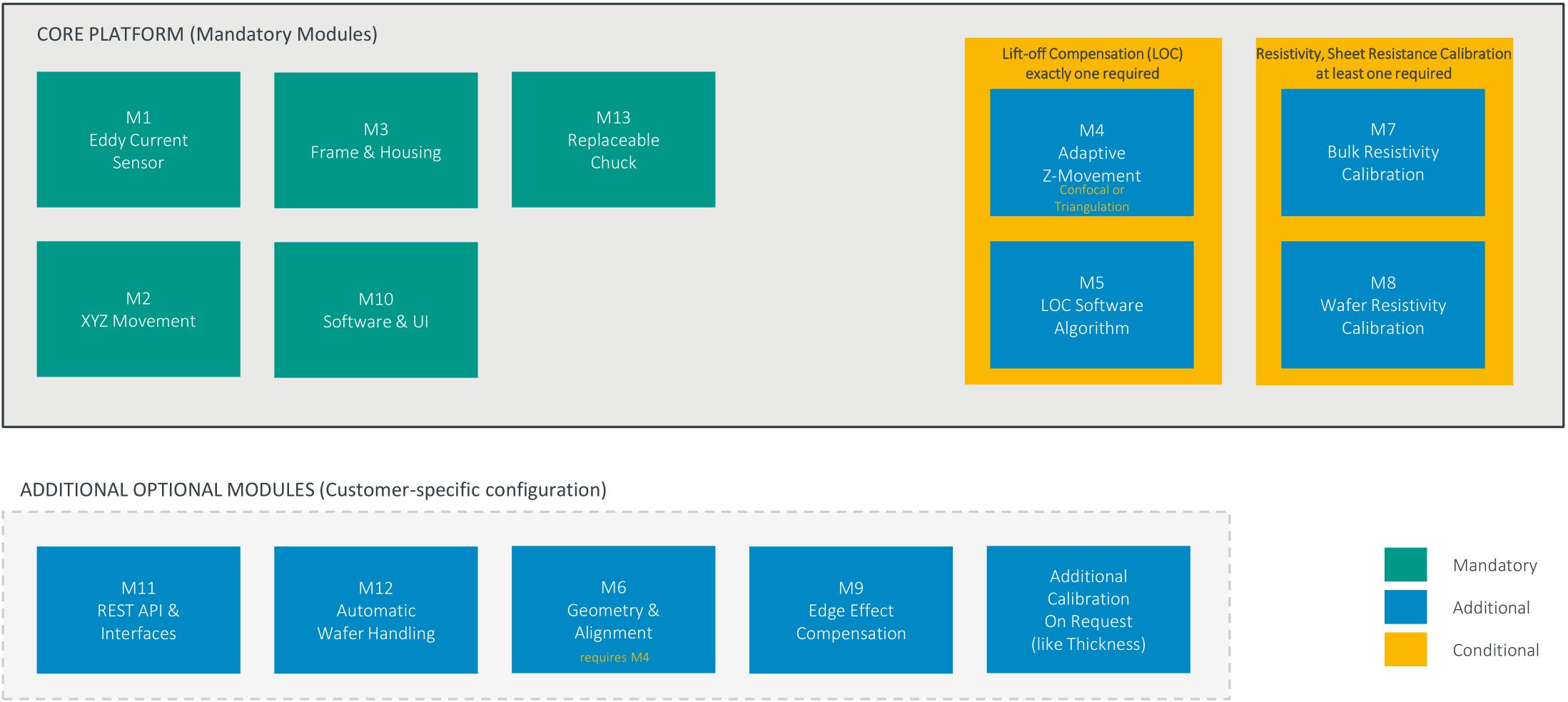
Modular Architecture of the EddyCus® map 8060 RMT
Eddy Current Sensor Module
- ASU Gen2 sensor with advanced signal processing
- Fast trigger board for high-speed data acquisition
- Data rate: up to 600 kHz trigger rate
- Effective measurement rate: 150 points/second
- Non-contact, non-destructive measurement
- Suitable for conductive thin films and bulk materials
Key Benefits
- No sample preparation required
- 100% non-destructive — measure production wafers
- High repeatability < 0.1% (1σ)
- Fast data acquisition for high throughput
High-Precision Linear Motor Axes
- Linear motor axes for X, Y, and Z movement
- Maintenance-free operation (no spindles/belts)
- High dynamics for fast scan speeds
- Encoder-triggered measurement for precise positioning
| Axis | Travel Range | Accuracy |
|---|---|---|
| X-Axis | 800 mm | < ± 15 µm |
| Y-Axis | 600 mm | < ± 15 µm |
| Z-Axis | 150 mm | < ± 5 µm |
Key Benefits
- True position accuracy for reliable mapping
- High scan speed → higher throughput
- No mechanical wear → long lifetime
- Precise Z-control for adaptive scanning
Robust Industrial Platform
- Ready for automated wafer handling add-on (Module 12)
- Complete measurement system housing
- Integrated frame for all mechanical components
- Vibration-damped construction
- Front-loading access for easy sample handling
- Status LEDs and optional display
Key Features
- Compact footprint for lab environments
- Safety interlocks on all access doors
- Emergency stop (E-Stop) functionality
- Handler port for automation integration
Adaptive Z-Movement
Required for samples with warp > ± 200 µm
Two-Pass Measurement Principle
- Pass 1: Topography scan captures surface profile
- Pass 2: Z-axis follows surface for constant working distance
- Improves accuracy on warped samples
- Superior to software-based lift-off compensation
Key Benefits
- Best possible accuracy on warped wafers
- Measure samples with high bow/warp
- Constant working distance → consistent results
- Enable TTV measurement (with confocal, for semi-transparent samples)
Lift-off Compensation Algorithm (LOC)
Required if Module 4 (Adaptive Z) is not selected
Software-Based Distance Compensation
- Algorithm compensates for lift-off variations
- Uses eddy current signal characteristics
- Suitable for samples with warp ≤ ± 200 µm
- Single-pass measurement (faster throughput)
- Cost-effective alternative to adaptive Z
How It Works
The LOC algorithm analyzes the raw data characteristics of the eddy current signal to mathematically compensate for variations in sensor-to-sample distance during a single-pass scan.
Key Benefits
- Faster measurement (single pass)
- Lower system cost
- Good accuracy for flat samples
- No additional hardware required
Geometry and Alignment Detection
Requires Module 4 (Adaptive Z-Movement)
Automatic Wafer Orientation & Geometry Analysis
- Automatic flat and notch detection
- Precise wafer rotation angle measurement
- Sample diameter measurement
- Roundness/circularity analysis
- Alignment marker detection
Measured Parameters
| Parameter | Typical Accuracy |
|---|---|
| Rotation Angle | ≤ 0.5° |
| Flat/Notch Position | Automatic detection |
| Diameter | < 0.1 mm |
| Roundness | Deviation from ideal circle |
Key Benefits
- Automatic wafer orientation detection
- Correct data alignment to crystal orientation
- Quality control of wafer geometry
Calibration for Sheet Resistance / Bulk Resistivity
NIST-Traceable Calibration for Thick Samples
- NIST traceability / conformity certified
- For bulk materials ≥ 3× standard penetration depth (e.g., min. 3 mm @ 1 mΩ·cm)
- Global calibration for samples ≥ 125 mm diameter
- Customer-selectable measurement pitch
Edge Cut-off by Resistivity
Measurement valid from edge cut-off distance inward:
| Resistivity | Edge Cut-off |
|---|---|
| 11 mΩ·cm | 9 mm |
| 25 mΩ·cm | 10 mm |
| 117 mΩ·cm | 12 mm |
| 1049 mΩ·cm | 18 mm |
For measurement up to the edge please order Module 9 (EEC)
Key Benefits
- Traceable, certified measurements
- Comparable results across systems
- Compliance with quality standards
Wafer Resistivity Calibration
For Thin Samples Below Standard Penetration Depth
- Calibration for samples < 3× standard penetration depth
- Multidimensional SURAGUS calibration enables
interpolation for any desired thickness - Works with known thickness or measured thickness
- For SiC wafers: thickness from confocal sensor (Module 4)
Workflow
- Specify or measure wafer thickness
- System calculates skin depth correction
- Calibration accounts for finite thickness effects
- Output: True resistivity values
KEY BENEFITS
- Accurate resistivity for thin wafers
- Combined thickness + resistivity analysis
- Automated workflow with confocal sensor
Edge Effect Compensation (EEC)
Measurement Down to 1 mm from Sample Edge
- Universal algorithm for edge correction
- Valid measurements as close as 1 mm to edge
- Global algorithm for samples ≥ 125 mm diameter
- Eliminates edge exclusion zones
- Full wafer utilization in mapping
Coverage Comparison
| With EEC | Without EEC | |
|---|---|---|
| Edge exclusion | 1 mm | 9 – 18 mm (varies) |
| Usable area of a 200 mm wafer | ~99 % | ~85 % |
| Edge defect detection | Full coverage | Limited |
Key Benefits
- Full wafer coverage
- Detect edge-related process issues
- Maximize usable wafer area
Software and User Interface
“Imaging Control” — Next-Generation Software Platform
Core Features
- Modern, intuitive user interface
- Recipe management with version control
- Real-time measurement visualization
- Comprehensive data analysis tools
- Multiple scan path options (meander, circular)
Data Management
- InfluxDB time-series database
- ASCII data export
- Automated PDF reporting
Analysis Capabilities
- 2D resistivity mapping
- Statistical analysis (mean, σ, uniformity)
- Line scan / profile extraction
- Histogram analysis
- Customizable report templates
REST API and Interfaces
Full Automation & Integration Capabilities
REST API Endpoint Groups
| Function Group | Description |
|---|---|
| System status | Device status, version, connection health |
| Recipe management | CRUD operations, parameter validation |
| Measurement control | Start, abort, progress tracking |
| Sample handling | Load/unload commands for automation |
| Results & data | Maps, timeseries, statistical results |
| Calibration | Calibration data, reference measurements |
| Reporting | PDF generation, data export |
Integration Interfaces
- Process Output Files (PO-Files) for MES
- SECS/GEM (semiconductor standard)
Key Benefits
- Full remote control capability
- Integration into existing IT/OT systems
- Automated data flow to MES/ERP
- OpenAPI/Swagger documentation
Automatic Wafer Handling Add-on
Compact Automation for High-Throughput Applications
- Extremely compact side-mounted module
- SCARA robot for precise wafer handling
- Supports 100 mm to 300 mm wafers
- Open cassette interface (standard)
- Seamless integration with M3 housing
Specifications
| Parameter | Specification |
|---|---|
| Wafer sizes | 100, 150, 200, 300 mm |
| Cassette type | Open cassette |
| Throughput | Optimized for measurement time |
| Placement accuracy | < 1 mm |
Key Benefits
- Unattended cassette-to-cassette operation
- Consistent wafer placement
- Reduced operator dependency
- Higher effective throughput
Replaceable Chuck System
Quick-Change Sample Holders for Different Applications
- Tool-free chuck exchange
- Optimized for specific wafer sizes
- Non-conductive materials (PEEK, PVC, Acrylic)
- Precision alignment features
- Sample fixation for high scan speeds
Available Chuck Configurations
| Type | Sizes / Dimensions |
|---|---|
| Wafer chuck | 100, 150, 200, 300, 350 mm |
| Panel chuck | Custom sizes up to 600 x 600 mm |
Key Benefits
- One system for multiple sample types
- Fast changeover between applications
- Optimized holding for each size
- Future-proof for new sample formats